PWB vs. PCB: How To Differentiate The Two
We will compare PWB vs. PCB to learn the differences in this article.
We will compare PWB vs. PCB to learn the differences in this article.
PWB and PCB are often used interchangeably in the electronics industry, but the two don’t refer to the same thing.
Although, it is vital to note that the difference is in the technicalities.
But we won’t spare any details. So here is a detailed comparison of these two electrical boards.
What Is a PWB?
PWB is an acronym for Printed Wiring Board, and it refers to an epoxy glass substrate used to make interconnections between circuit components.
This definition seems similar to a PCB, but here’s the clarification.
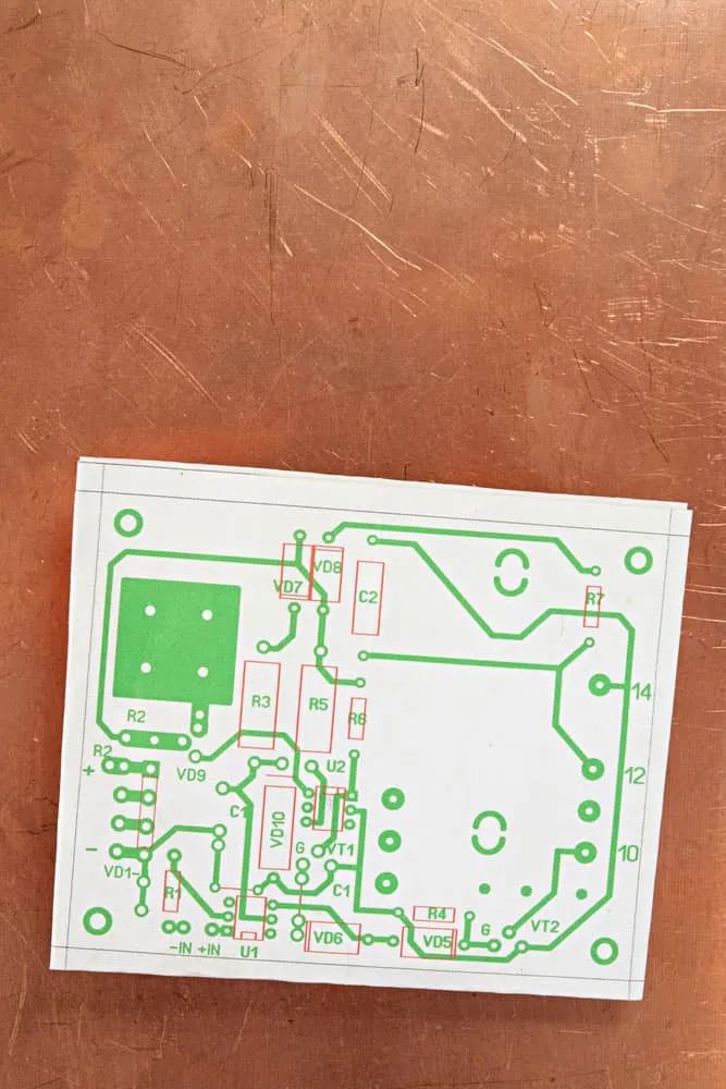
The PWB manufacturing process is more manual. So whenever you make a DIY PCB, you are building a PWB.
And the fabrication process involves using an etchant bath to create PCB from a metal-clad laminate to leave the circuit’s electrical and signal paths.
But before the etching step, you must draw the circuit, which was manual at first.
However, you can use a computer to draw a simple electronic circuit design, then etch it manually.
And whenever you do something manually, you cannot make it sophisticated.
So PWBs are simple PCBs that are usually either double or single-sided boards that can hold few components.
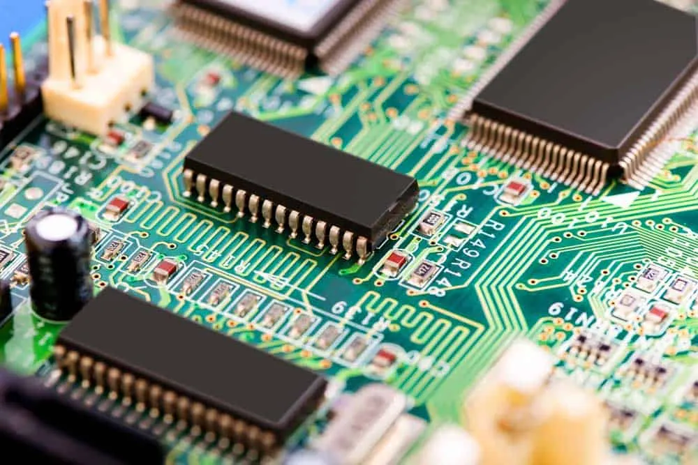
What Is a PCB?
But the foundation of these electronic products is similar to PWBs because their base is an insulating board (usually FR4). Some can have flexible substrates to suit a bending application area.
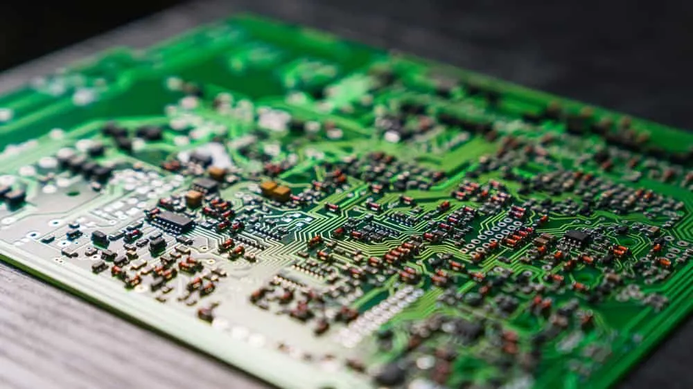
Using computers and machines to design and manufacture PCBs makes them more complex because they can have multiple conductive layers, with vias interconnecting them.
It is impossible to achieve this sophistication with PWBs due to the manual fabrication process.
PWB vs. PCB: Complexity
The primary difference between the two is complexity. PWBs are simplified versions of PCBs.
The term PWB came into existence in the early days of electronics manufacturing.
And the name was appropriate because the boards had electrical connections that traveled from point to point, similar to what you’d get when using wires.
So the technology transferred wires to boards by printing them on dielectric substrates, hence the name printed wiring board.
The term PCB emerged later when the PWB technology advanced and provided more complex functions.
Also, they have thinner traces, emit heat more efficiently, and bear more features that suit modern, high-performance electronic devices.
So currently, PWB refers to boards in pre-production or the ones you make as DIY projects at home.
PWB vs. PCB: Location/Area
The usage of the two terms also depends on the geographic location.
For instance, Americans interchange the two terms when referring to any printed wiring or circuit board. But they mostly use PCB.
On the other hand, the Japanese prefer using the term PWB because they associate PCB more with polychlorinated biphenyls, a toxic and carcinogenic chemical compound.
So electronic articles, documents, and journals meant for the Japanese market will most likely have the term PWB.
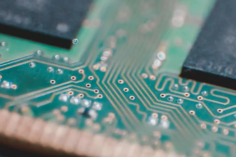
PWB vs. PCB: Materials
PWBs and PCBs utilize different materials in their construction. Some are similar, but others differ. So let’s consider these materials layer by layer.
Conductive Layer
The conductive layer must consist of an electrically conductive metal with minimal resistance.
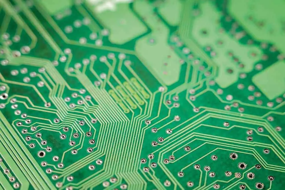
So both PWBs and PCBs use copper tracks to transmit power and signals around the board.
You can stick pre-made copper strips in the board or use an etching solution (chemical bath) to etch them from copper-clad laminates.
Insulation/Non-Conductive Layer
This layer separates and holds the conductive tracks in place while insulating them. And the most typical material is FR4, a glass-reinforced epoxy laminate.
However, the material might not provide sufficient dielectric performance for high-power or high-frequency applications.
So some PCBs can have other materials like ceramic in their non-conductive layers.
But PWBs are not complex boards. So they usually have an epoxy glass substrate, which provides enough dielectric performance for the circuit.
Prepreg
The prepreg assists the board’s core non-conductive layer to hold the layers in place.
Since PWBs are simple circuits with at most two layers, they usually don’t have prepregs.
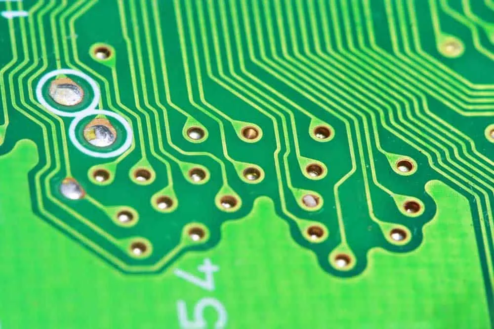
Solder
The solder used to mount electrical components in these two boards is the same. You can use solder paste or wire to assemble through hole or surface mount components on them.
Protective Coat/Conformal Coating
Copper oxidizes over time when exposed to the atmosphere. So it needs a protective coat to preserve the metal, which helps maintain its electrical properties.
Manufacturers usually use materials like gold, silver, nickel, and tin to cover the outer conductive layer in PCBs.
But most PWBs don’t have protective coats because they are pre-production units or are for DIY projects.
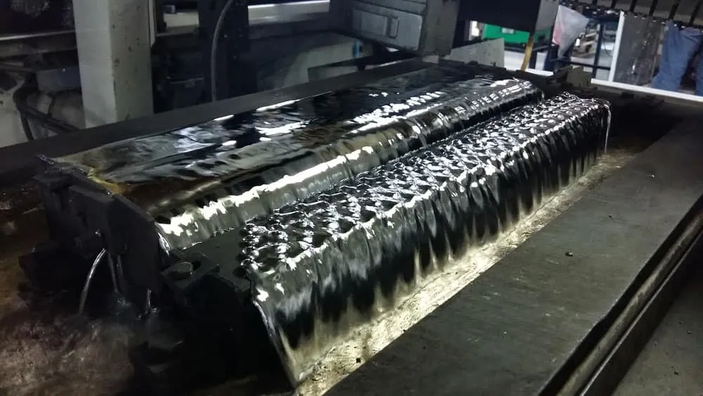
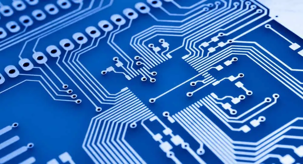
PWB vs. PCB: Fabrication
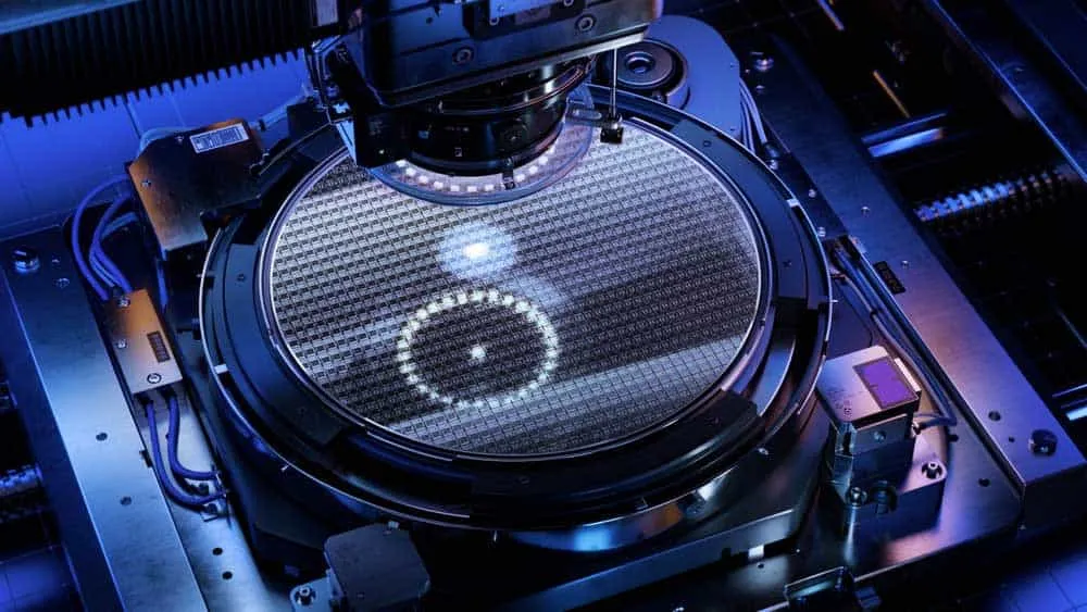
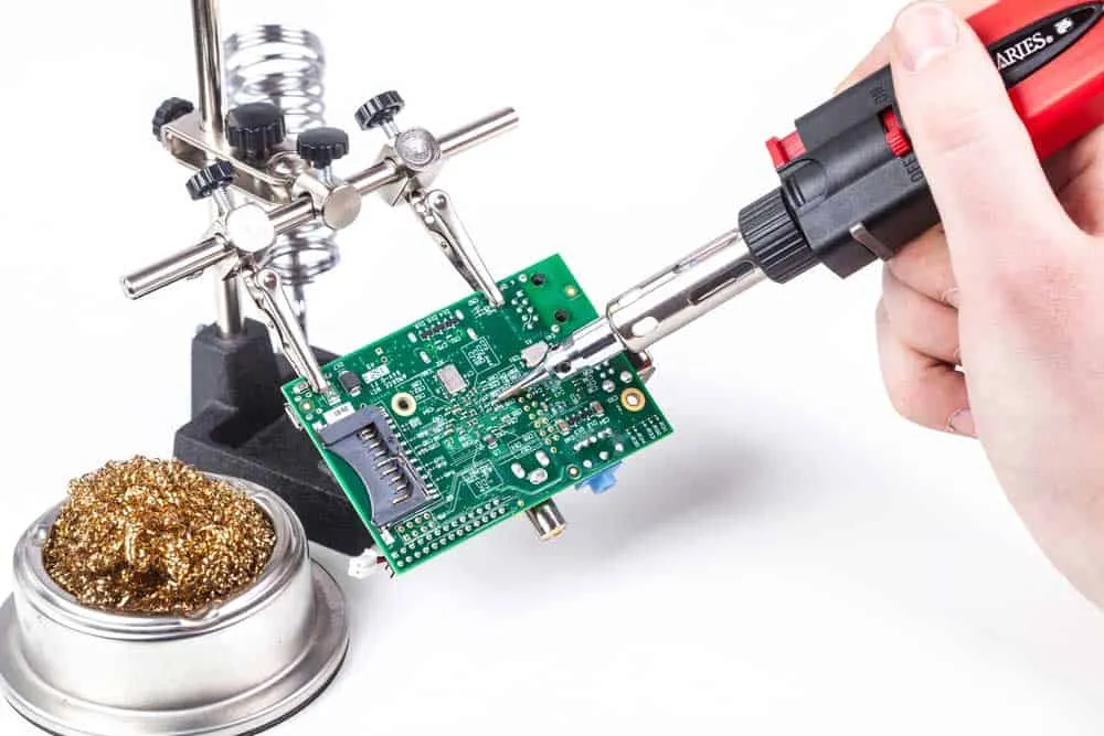
Fabricating a PWB is a relatively straightforward process that you can do at home. Check out this guide to make one. But developing a PCB is a more complex process.
Although it also encompasses circuit design as the first stage (like with PWBs), PCB design is more complicated and requires advanced CAD software.
And the designer must consider factors like impedance, routing, and trace separation when laying out the stack.
The copper patterning and etching processes are the same on both boards.
But multi-layer PCBs require lamination on the entire board surface to place the other conductive traces.
Also, they need plating, coating, solder mask/resist application, and silkscreen layering.
If you want to install through-hole components, drill either board to install the electrical component leads.
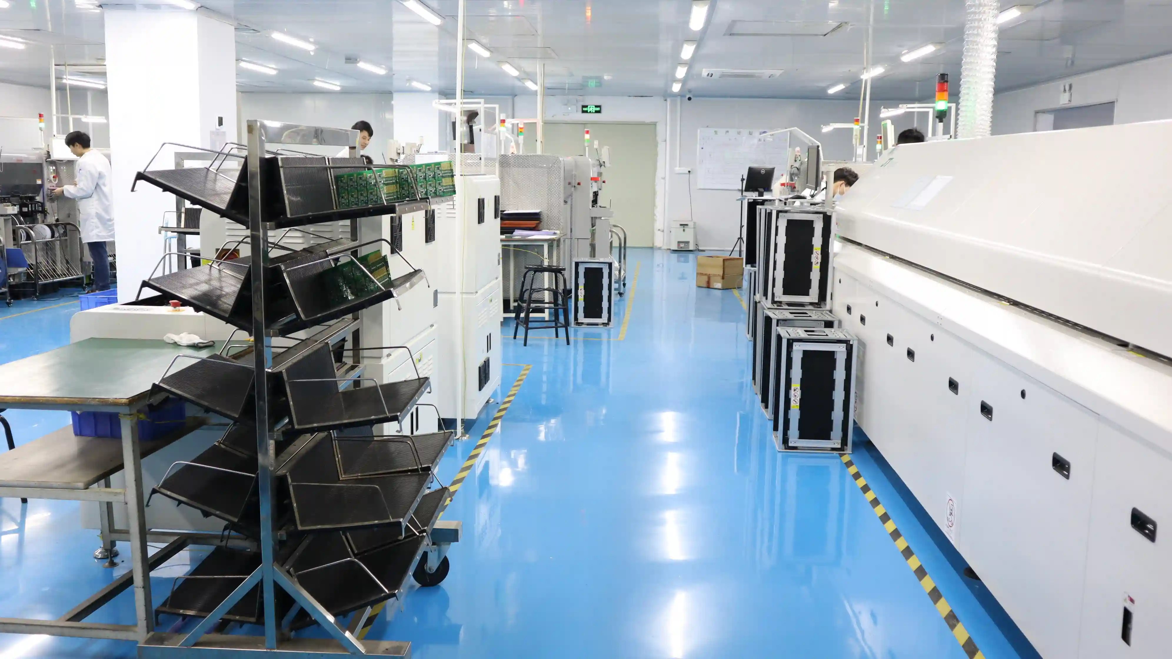
PWB vs. PCB: Assembly Process
When you order a PCB, you can include assembly in the product order to get it as a PCBA.
If this is the case, the board undergoes professional electronic component assembly using automated processes like:
- - Automated electronic component placement
- Reflow soldering for attaching surface mount components
- Wave soldering for installing through-hole components
- Inspection and testing
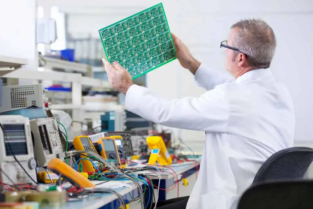
Alternatively, you can order a blank PCB and assemble it using a solder iron or gun. But with PWBs, the only option is manual soldering using a solder gun or iron.
Wrap Up
A thin line separates PWBs from PCBs because both refer to circuits printed on a non-conductive board as the base layer.
The primary difference is in their complexity. Printed circuit boards began as printed wiring boards when engineers started “miniaturizing” circuits from wires.
So some people view PCBs and PWBs as the same thing because the former is a newer generation of the latter. But others consider them separate entities.
That’s it for this article. Comment below to let us know what you think about the comparison. We appreciate your feedback. Check out our PCB manufacturing and assembly services for your projects.
Related Articles
Continue exploring similar topics
Turnkey PCB Assembly
We'll discuss turnkey PCB assembly in this article. Time is money, and you will most likely waste precious time handling some tasks in the PCB assembly process.
How to Surface Mount Solder
Every electronic circuit board you interact with features hole components and surface mount devices. But do you know how to surface mount solder components?
PCB Assembly Drawing
Learn what a PCB assembly drawing includes and why it matters. Understand key elements like component placement, polarity marks, and reference designators.
Ready to bring your PCB design to life?
Get an instant quote for your custom PCB fabrication and assembly needs.
Get Instant Quote