How To Make a PCB at Home: DIY Guide
This is a guide on how to make a PCB at home. While getting a PCB made by a manufacturer is relatively inexpensive nowadays, you can still build simple circuit boards.
This is a guide on how to make a PCB at home.
While getting a PCB made by a manufacturer is relatively inexpensive nowadays, you can still build simple circuit boards. It will be cheaper, and you’ll get the product quickly while sharpening your skills.
But if you don’t know where to start, here’s how to make a PCB at home. Read on to learn more about the process and steps.
How To Make a PCB at Home
You will need the following materials.
- - Thermal transfer paper
- Copper-clad laminate (copper plate)
- Ferric chloride solution
- Acetone
- Sandpaper or steel wool
- Beaker or glass bowl
- Tweezers
- Brushes
- Gloves
- Electric drill
- Laser printer
- Electric iron
- Soldering iron
- Solder wire
- Through-hole components
- Computer with a PCB design software
Please note that you can only use a laser printer for this process because it uses toners to print on paper.
The method we’ll use to make the board is known as the toner transfer method. It involves printing the layout design on special paper (thermal transfer paper). After that, we’ll transfer this toner to the copper layer via heat transfer.
Unlike ink, paper does not absorb toner. Instead, the toner powder forms a layer above the surface. So during heat transfer, the toner will move from the thermal paper to the copper plate.
Step 1: Design The Circuit
Use your preferred PCB design software to prepare the PCB layout. This layout design should connect the electronic components according to the circuit schematic design (circuit diagram).
Step 2: Printing
Once the PCB layout is complete, transfer the design to your printer to get it on paper. But you need to do some settings first. Click on the print menu and edit these settings.
- - Paper: A4
- Area: Full
- Orientation: Portrait
- Printer: PDF (Print To File)
- Alignment: Top left
- Scale Factor: 1
- Page Limit: 0
- Check “solid” and “black” boxes
Step 3: Cut the Copper Sheet
Cut the copper-clad laminate to match the layout size. Leaving a tiny margin around the layout design in step 2 will help you reduce wastage when cutting this copper layer.
So mark the boundaries using a sharp tool, such as a box cutter, then cut it out using a saw.
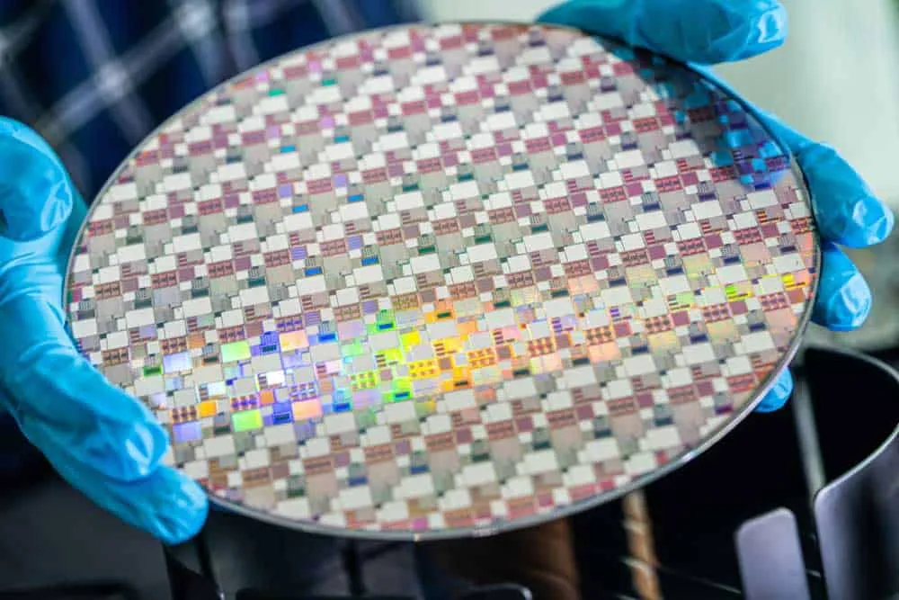
In this case, we’ll use a single-layer copper board to make a single-layer PCB. Double and multi-layer boards are ideal for building complex circuits, and making them is more challenging. So we won’t touch them for now.
Step 4: Clean the Copper Layer
Use steel wool or sandpaper to polish the copper board copper surface. This action smoothens the layer, scrubs the upper oxide layer to expose the copper, and removes any other impurities.
Fingerprints and dirt are typical to find above the copper. Polishing removes these, as well.
But the sandpaper or steel wool should not be too harsh to remove the copper. Also, be gentle but thorough. If well done, you should have a smooth, shiny surface. Remember to sand the edges if they are rough.
After that, clean the PCB using acetone or alcohol to remove the tiny powder and copper deposits from the surface.
Step 5: Transfer the Design Drawing
Place the circuit printout on the board with the printed side facing the copper surface.
You can use the heatless toner transfer process to move the toner to the copper layer, but this method requires chemicals.
So we’ll use heat transfer using an iron box because it is safer.
Preheat the iron box to around 200°C, which should be between linen and cotton on the temperature control knob. Once hot, iron the paper above the copper-clad laminate slowly.
One of the indicators that can show you the process is complete is when the paper begins changing color. The heat burns the thermal transfer paper, changing it from white to yellow.
After ironing, place the board and paper in a bowl of cold water. Copper is an excellent conductor of heat, so be careful when handling it after ironing. It will be hot.
When dipped in water, the instant cooling will create a stronger bond between the toner and copper. Let it sit in water for about two minutes, then unwrap the paper.
You can use the water to remove the stuck paper. But scrub lightly to avoid removing the toner. You can use a permanent marker to repair tiny sections that did not transfer the design properly.
Step 6: Etching
Transferring the toner in the step above effectively creates a protective layer that will prevent etching or corrosion using an etching solution.
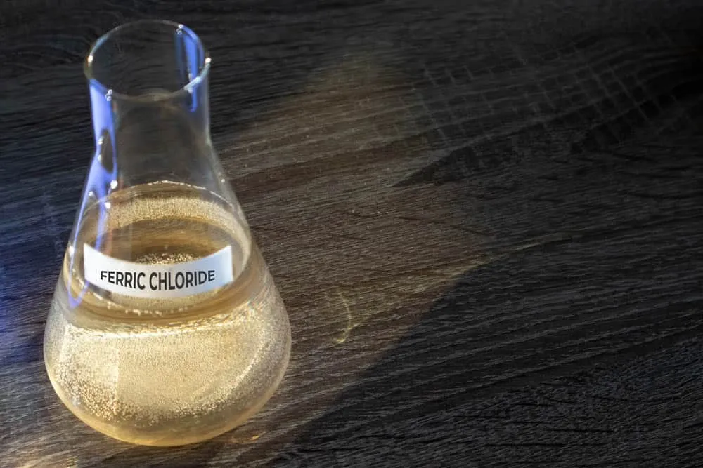
And we’ll use a ferric chloride solution for this process. You can dissolve ferric chloride powder in water to make this solution or buy a ready-made solution.
The liquid is toxic and harmful to the body. So handle it with care. Wear gloves and use tweezers.
Ferric chloride will not react with toner because it contains carbon as the primary material. So when you remove the board and place it in clean water, all the unmasked copper will be out. Clean the board using water to eliminate all the remaining acid.
Step 7: Remove the Black Toner
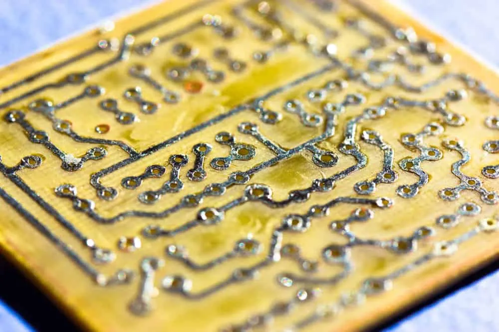
At this point, the circuit will be ready but hidden under the toner. So scrub the conductive lines using mild emery paper or acetone/alcohol and steel wool. The result should be shiny copper traces.
Step 8: Drill PCB Holes
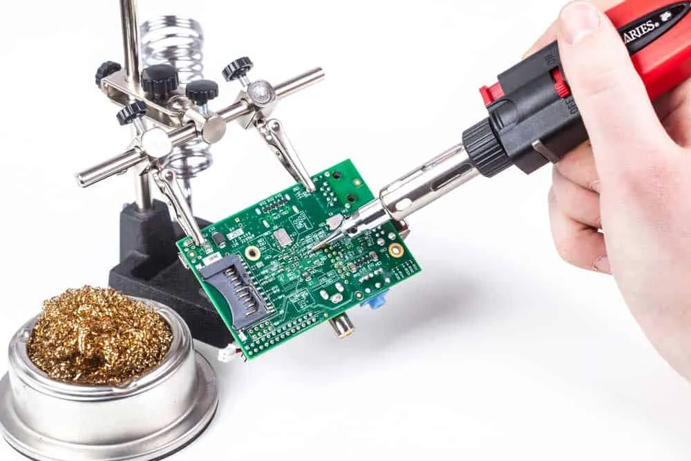
Step 9: PCB Assembly
Mount your through-hole components on the other side of the board, then solder them to the copper traces via the protruding leads.
Step 10: Testing
Test the assembly to see if power moves through the circuit as required. If everything works, you are good to go.
Pros of DIY Circuit Boards
- - Quick production
- Affordability
But making one PCB for prototyping will be costly due to the low economies of scale. So making the board at home is cheaper, especially if it is not complex.
Cons of DIY Circuit Boards
- - Cumbersome manufacturing process
- Low efficiency
- Zero quality guarantees
- You might have difficulty finding all the materials
Wrap Up
Making a PCB at home isn’t such a difficult task after all. Getting all the required items might be challenging, but it is fun after that (if you enjoy working on electronics).
Contact us or comment below if you want to make your first PCB at home. We’ll be happy to help. For professional-quality boards, explore our PCB manufacturing services and rapid prototyping.
Related Articles
Continue exploring similar topics
How to Identify Diodes
Learn how to identify diodes by type and polarity. Understand markings, use multimeter testing, and recognize common diode types for your electronic projects.
How to Solder Wires to a Circuit Board
Do you know how to solder wires to a circuit board? It is straightforward, but you must perform it correctly to ensure a perfect electrical connection.
How To Mix Ferric Chloride for Etching
Learn how to mix ferric chloride for PCB etching. Get the right ratios, safety tips, and step-by-step instructions for etching copper-clad boards at home.
Ready to bring your PCB design to life?
Get an instant quote for your custom PCB fabrication and assembly needs.
Get Instant Quote