THT Assembly Service
Through-Hole PCB Assembly for Connectors, Power Parts, and Mixed Builds
PCBInsider builds through-hole PCB assemblies where connector retention, thermal mass, solder access, and test evidence must be settled before the purchase order moves from RFQ to production.
ISO 9001:2015
Quality system context
IPC-A-610
Acceptance criteria
J-STD-001
Soldering process reference
24 hours
Complete RFQ review target
TL;DR
- Through-hole PCB assembly fits connectors, terminals, transformers, relays, and power parts that need stronger mechanical retention.
- Selective soldering is preferred when SMT parts, plastics, or nearby heat-sensitive components make full wave exposure risky.
- Quote-ready files should include Gerber, BOM, centroid, assembly drawing, IPC class, solder alloy, and test requirements.
- PCBInsider reviews hole fill, thermal relief, fixture access, and inspection evidence before releasing mixed-technology builds.
Capability Built Around Solder Access and Mechanical Risk
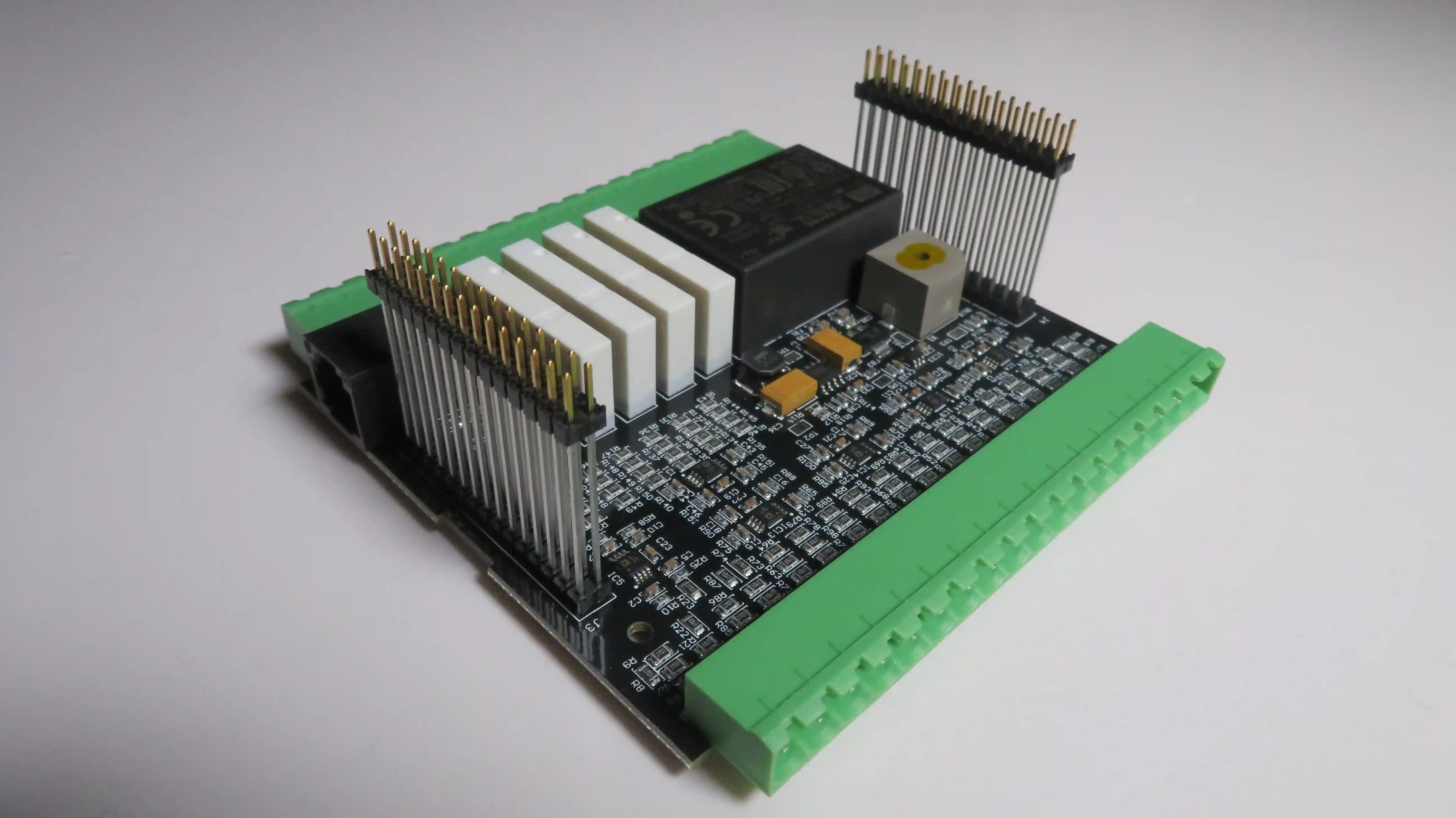
Through-hole assembly is not only a soldering step. Through-hole technology is an electronics assembly method that uses plated holes to anchor component leads; the process plan must account for heat, hole fill, and field stress before production.
THT and Mixed-Technology Assembly
Through-hole components can be added after SMT reflow so connectors, terminals, shields, relays, transformers, and large capacitors are installed without disrupting fine-pitch surface-mount work.
Selective and Wave Solder Review
Engineering chooses selective soldering, wave soldering, or controlled hand soldering according to connector spacing, thermal mass, solder-side clearance, pallet access, and board finish.
Connector Mechanical Support
Board-edge connectors, power-entry parts, terminal blocks, and headers are reviewed for pin fit, standoff height, retention features, cable load, and enclosure installation stress.
Inspection Evidence by Risk
Visual inspection, AOI where geometry allows, first article checks, continuity test, ICT, and functional test can be paired with IPC-A-610 Class 2 or Class 3 acceptance expectations.
NPI-to-Production Handoff
Prototype builds can start with controlled manual or selective soldering, then move into repeatable fixtures, documented recipes, and lot evidence as volume increases.
DFM for Hole Fill and Heat Balance
We check pad size, annular ring, plated-hole tolerance, copper-plane thermal relief, keepout around tall parts, and solder-side shadowing before the build reaches production.
Technical Scope and RFQ Boundaries
PCBInsider quotes through-hole PCB assembly from the actual release package, not from a generic connector count. IPC references such as IPC-A-610 and IPC-J-STD-001 matter when a buyer needs controlled evidence rather than visual approval alone.
Selective soldering is a localized soldering process for specific through-hole joints, and wave soldering is a full solder-wave process suited to boards designed for that exposure. The better choice depends on solder-side access, thermal mass, bottom-side SMT risk, and whether the board has enough repeated joints to justify fixtures.
| Service focus | Through-hole PCB assembly for connectors, power parts, mixed SMT/THT boards, and production electronics |
|---|---|
| Best-fit parts | Headers, terminal blocks, transformers, relays, electrolytic capacitors, shields, switches, sockets, and high-force connectors |
| Soldering methods | Selective soldering, wave soldering, controlled hand soldering, and process-specific fixture planning by review |
| Input package | Gerber or ODB++, BOM, centroid when SMT is included, assembly drawing, polarity notes, solder alloy, IPC class, and test plan |
| Quality references | IPC-J-STD-001 process expectations, IPC-A-610 finished assembly acceptance, ISO 9001:2015 quality-system discipline |
| Inspection options | First article inspection, visual criteria, AOI where accessible, X-ray by package risk, continuity, ICT, and functional test |
| Lead-time signal | 24-hour quote review for complete files; production timing depends on part availability, fixture needs, and test scope |
| Out of scope | Production release from incomplete drawings, unsupported connector strain, unapproved substitutions, or unclear Class 2/Class 3 criteria |
How We Choose the Soldering Path
A through-hole quote should identify why each process was chosen. PCBInsider treats selective soldering, wave soldering, and hand soldering as engineering choices tied to board geometry, volume, and acceptance evidence.
| Build condition | Likely process | Production reason |
|---|---|---|
| Many through-hole pins, open solder side, stable layout | Wave soldering | Efficient for larger THT populations when SMT exposure, pallet masking, and solder-side keepouts are controlled. |
| Mixed SMT/THT board with heat-sensitive nearby parts | Selective soldering | Local nozzle control reduces full-board thermal exposure and helps protect connectors, plastics, and bottom-side SMT parts. |
| Low quantity or engineering change risk | Controlled hand soldering | Useful for prototypes and ECO work, but the inspection plan must define acceptable fill, wetting, and rework limits. |
| High-force cable or enclosure interface | Mechanical review first | Connector load should be carried by housing, fasteners, or strain relief, not only by solder joints. |
| Class 3 or field-critical product | More evidence | Add first article records, recipe checks, IPC-A-610 criteria, and electrical test coverage before production release. |
The practical trade-off is cost versus repeatability. Hand soldering can be responsible for a 10-piece ECO lot, but a 1000-piece recurring order usually needs fixture thinking, solder recipe control, and inspection records so operator skill is not the only process control.
Production Flow
The process keeps DFM, soldering, inspection, and test records connected so a through-hole issue found in first article does not repeat through the lot.
1
RFQ and drawing review
Engineering checks the Gerber or ODB++ package, BOM, assembly drawing, IPC class, connector notes, polarity markings, solder alloy, and required test records before quoting.
2
DFM for THT solder access
The team reviews hole-to-lead fit, pad size, thermal relief, copper balance, solder-side clearance, pallet access, and whether selective soldering or wave soldering fits the board.
3
Kitting and process setup
Parts are verified, moisture-sensitive SMT items are controlled where present, fixtures or pallets are planned, and solder recipes are prepared for the approved process path.
4
SMT, insertion, and soldering
Boards move through SMT first when needed, then through-hole insertion, selective soldering, wave soldering, or controlled hand soldering according to the released traveler.
5
Inspection, test, and release
Finished assemblies receive first article checks, IPC-A-610 workmanship review, continuity or ICT where specified, functional test by requirement, and packaging controls before shipment.
Best-Fit Applications
Through-hole PCB assembly is strongest when the part must survive insertion force, cable pull, service handling, high current, or field replacement. It is less attractive when an SMT equivalent meets the same electrical and mechanical requirement with less board area.
Industrial controls with pluggable terminal blocks and relay outputs
Power conversion boards using transformers, large capacitors, and heat-heavy parts
Telecom and networking hardware with board-edge or high-retention connectors
Medical and laboratory electronics requiring documented assembly release
Automotive and transportation modules with harness interfaces and vibration exposure
Box build assemblies where the PCBA must mate cleanly with cables and enclosure hardware
Engineering Review
Reviewed by Hommer Zhao, PCBInsider founder and technical expert. Hommer works with PCB fabrication, PCBA sourcing, harness integration, and box build programs across industrial, medical, telecom, automotive, and embedded electronics projects.
Quality References
Relevant controls include ISO 9001:2015 quality-system discipline, IPC-A-610 Class 2 or Class 3 acceptance criteria, and IPC-J-STD-001 soldering process expectations when the purchase order requires formal workmanship evidence.
Transparent Quote Inputs
A complete RFQ can enter 24-hour review when Gerber or ODB++, BOM, assembly drawing, connector notes, solder alloy, IPC class, target quantity, and electrical test requirements are included.
FAQ: Through-Hole PCB Assembly Buying Questions
These answers are written for RFQ-stage buyers comparing process options, evidence requirements, and realistic handoff risk.
What is through-hole PCB assembly?
Through-hole PCB assembly is a board assembly process where component leads pass through plated holes and are soldered on the opposite side of the circuit board. It is common for connectors, transformers, relays, terminal blocks, electrolytic capacitors, and mechanically stressed parts. PCBInsider usually combines THT with SMT on mixed-technology builds, then applies IPC-A-610 acceptance criteria and IPC-J-STD-001 soldering expectations according to the buyer's requested class.
Should my mixed SMT and through-hole board use selective soldering or wave soldering?
Selective soldering is usually safer when a mixed SMT and through-hole board has bottom-side SMT parts, heat-sensitive plastics, dense connectors, or tight keepout areas. Wave soldering can be efficient when the solder side is open and the through-hole population is high. During RFQ review, PCBInsider checks solder-side clearance, pallet access, thermal mass, hole fill risk, and IPC-A-610 class before recommending one process path.
A typical robotics PCBA rollout uses a multi-PO program with split deliveries, same-day payment confirmation, and a proactive delivery-risk alert for constrained orders. That kind of schedule visibility matters when through-hole work, sourcing, and final test must land in separate delivery windows.
I need 200 through-hole PCB assemblies for an industrial pilot. Is that too small?
A 200-piece through-hole PCB assembly pilot is a normal NPI quantity, especially when connector fit, enclosure installation, or test coverage still needs proof. For low-volume builds, controlled hand soldering or selective soldering may avoid unnecessary wave fixtures. The quote should still define solder alloy, IPC class, inspection method, and functional test coverage so the 200 units can become a repeatable production baseline instead of a lab-only build.
What files do you need to quote THT assembly accurately?
A quote-ready THT assembly package should include Gerber or ODB++ files, BOM with manufacturer part numbers, assembly drawing, polarity and orientation notes, solder alloy requirement, acceptable IPC class, test plan, and target quantity. If SMT is also included, send centroid data and stencil notes. Missing connector drawings, alternate part rules, or test requirements can add 1 to 3 clarification cycles before pricing is reliable.
How do you inspect through-hole solder joints?
Through-hole solder joints are inspected against the released workmanship class, commonly IPC-A-610 Class 2 or Class 3. Inspectors check wetting, hole fill, solder bridges, skipped joints, lead protrusion, lifted pads, flux residue, and connector seating. AOI may help on accessible geometry, but visual inspection and first article review remain important for tall connectors and shielded areas. ICT or functional test adds electrical evidence when the board design provides test access.
Can through-hole PCB assembly include box build or cable integration?
Yes, through-hole PCB assembly can continue into wire harness connection, enclosure installation, firmware loading, labeling, and final functional test. This is common when board-mounted connectors define the mechanical interface to the product. For best results, include torque values, mating connector drawings, cable strain relief requirements, and final test limits in the release package. Connector solder joints should not carry cable pull or enclosure stress by themselves.
When should I avoid through-hole components?
Avoid through-hole components when SMT alternatives can meet the current, voltage, mechanical, and service requirements with lower assembly cost and better routing density. THT is still the better choice for many high-force connectors, large power parts, and field-serviceable interfaces. The decision should compare board area, insertion labor, solder process, test access, and expected mechanical load rather than treating through-hole parts as automatically stronger.
Related Services
Most through-hole programs connect to upstream SMT planning, stencil decisions, component sourcing, and electrical test coverage.
PCB Assembly
Broader SMT, through-hole, BGA, and mixed-technology assembly coverage.
Learn moreSMT Assembly
Surface mount assembly before through-hole insertion and final soldering.
Learn morePCB Stencil Service
Stencil strategy for mixed builds where SMT paste printing drives first-pass quality.
Learn moreICT Testing Service
Fixture-based electrical screening for production lots with enough test access.
Learn moreGet a Quote for Through-Hole PCB Assembly
Send the Gerber package, BOM, assembly drawing, connector notes, IPC class, and test plan. We will review soldering method, fixture needs, and release evidence before quoting the build.