Hard-Gold Edge Connector PCB Support
Gold Finger PCB Manufacturing for Edge Connector Boards
PCB Insider builds gold finger PCBs for plug-in cards that need hard-gold contact control, bevel geometry review, finished thickness discipline, and assembly handling that protects the edge connector surface from first article through repeat production.
Hard Gold
Wear Surface for Card Edges
30-45 deg
Common Bevel Review Range
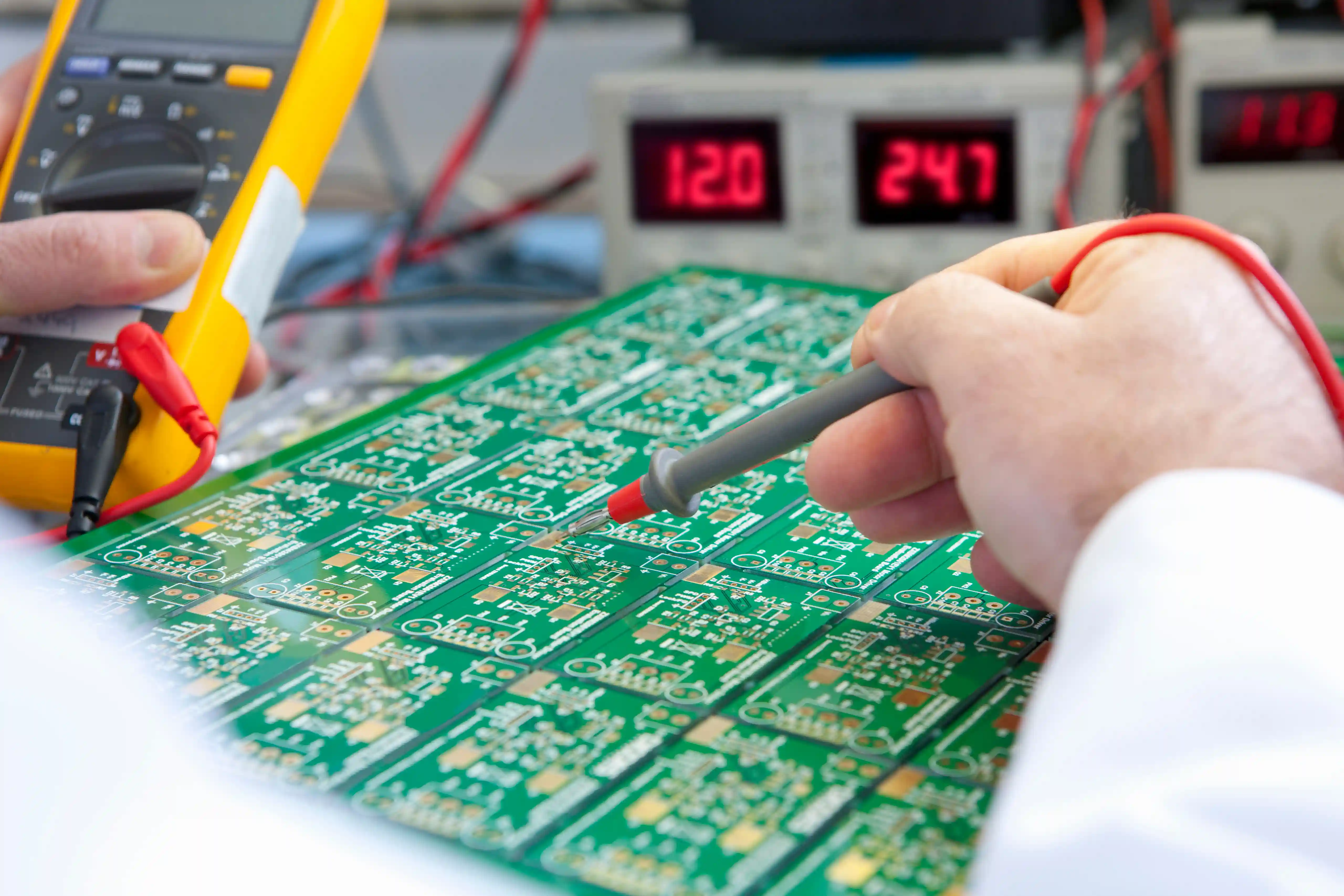
100%
Electrical Test Available
IPC Review
A-600, 6012, A-610, J-STD-001
Why Gold Finger PCBs Need a Separate Manufacturing Review
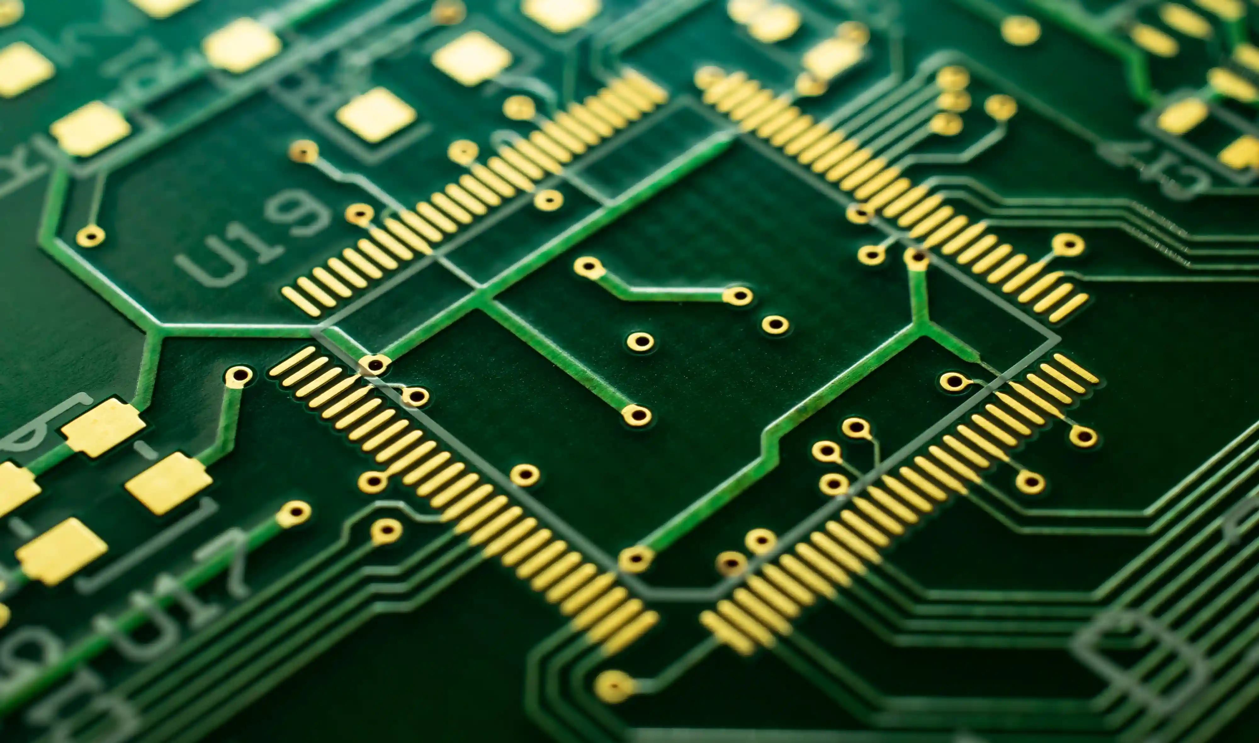
A gold finger PCB is a printed circuit board with plated contacts on the board edge, usually designed to slide into a card-edge connector. The manufacturing risk sits at the boundary between fabrication and mechanics: IPC-6012 fabrication rules, IPC-A-600 visual acceptance, hard-gold plating notes, and connector tolerances all affect whether the board seats cleanly.
The page is narrower than general PCB manufacturing. It is written for buyers whose RFQ includes card-edge fingers, PCIe-style contacts, industrial I/O boards, test adapters, or backplane daughtercards where hard gold, beveling, and contact cleanliness decide product reliability.
Hard-Gold Edge Connector Review
Gold finger PCBs are checked as mechanical interconnects, not only as fabricated boards.
Finished Thickness and Bevel Control
Card-edge connectors are sensitive to board thickness and entry geometry.
Plating Stackup Planning
Hard-gold fingers require a plating callout that separates the wear area from ordinary solderable finishes.
Surface and Edge Inspection
Finished fingers are inspected for nicks, exposed copper, staining, burrs, plating skips, mask encroachment, and rough bevel transitions.
Assembly-Aware Handling
If the board is populated after fabrication, the gold finger area needs protection from flux, scratches, tape residue, and handling marks.
RFQ Documentation Cleanup
Many gold finger RFQs stall because the drawing says only "gold finish." We help clarify whether the buyer needs ENIG, selective hard gold.
Gold Finger PCB Capability Snapshot
Service focus
Gold finger PCB manufacturing for hard-gold card-edge and edge connector boards
Best-fit products
PCIe-style cards, memory-style modules, industrial controllers, test adapters, plug-in I/O cards, backplane daughtercards
Surface finish approach
Selective electroplated hard gold over nickel for wear contacts; ENIG, OSP, or HASL lead-free elsewhere by drawing
Bevel guidance
30-45 degree bevel commonly reviewed against connector data sheet and finished board thickness
Board types
Rigid FR-4, high-Tg FR-4, selected HDI and controlled-impedance boards by application review
Fabrication controls
Finished thickness check, finger alignment, mask pullback, hard-gold callout, edge profile, and electrical test
Assembly handoff
SMT, through-hole, selective soldering, AOI, X-ray, and box build support when the edge connector board is populated
Release files
Gerber or ODB++, drill file, fabrication drawing, connector data sheet, BOM, centroid, and assembly drawing if populated
Commercial path
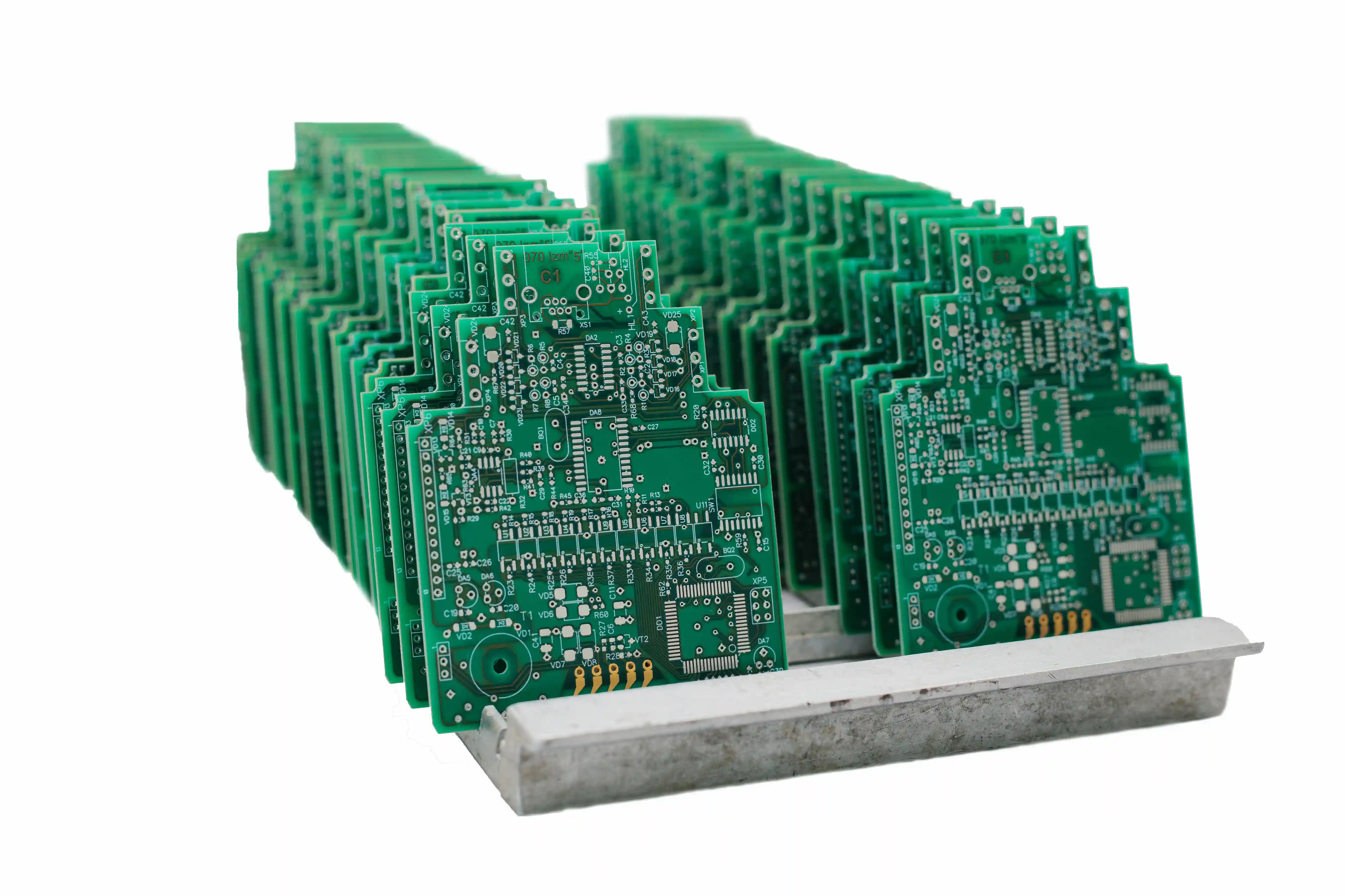
Prototype, 200-piece pilot lots, NPI builds, and repeat production after first-article approval
Out of scope
Unspecified decorative gold, uncontrolled manual edge sanding, or undocumented connector substitutions
Hard-gold thickness, nickel thickness, and finished edge tolerance should come from the product requirement or mating connector data sheet. When the RFQ does not define those values, PCB Insider flags the gap before production release instead of guessing.
Buyer Priorities
Gold thickness is a design decision
The right hard-gold callout depends on insertion cycles, connector force, contact geometry, and cost target.
Bevel geometry must match the socket
A square board edge can damage the connector or make insertion unreliable.
Panel strategy affects contact quality
Tabs, rails, and final routing should avoid damaging the finger area.
Inspection evidence speeds approval
For NPI programs, buyers often need first-article photos, electrical test records, and dimensional notes on the edge connector area before they approve.
Manufacturing Workflow for Hard-Gold Edge Connectors
Gold finger PCB manufacturing works best when the connector requirement is treated as an RFQ control point. The workflow below connects drawing review, hard-gold plating, bevel planning, inspection, and optional PCB assembly so the contact area is not damaged after fabrication.
Step 1
Confirm connector mechanics
We review the mating connector data sheet, finished PCB thickness, finger length, pitch, keying, bevel side, and keepout region.
Step 2
Lock plating and finish notes
Engineering checks whether the drawing calls out selective hard gold over nickel, ENIG elsewhere, solder mask pullback, and the exact contact area.
Step 3
Plan panel, profile, and bevel sequence
The panel plan protects the card-edge area through fabrication, plating, routing, beveling, and test.
Step 4
Fabricate, inspect, and electrically test
Boards move through normal PCB fabrication plus selective plating and edge finishing.
Step 5
Assemble or release bare boards
Bare gold finger PCBs can ship after inspection, or continue into SMT, through-hole, programming, test, and box build.
Hard Gold, ENIG, and the Cost Trade-Off
Hard gold and ENIG are often confused because both expose a gold surface. ENIG is a solderability finish for pads, while electroplated hard gold is a wear surface for repeated connector insertion. The right answer depends on the contact life target, not on appearance.
For a single-use programming tab or low-cycle debug connector, buyers sometimes choose a lighter finish strategy after reviewing the risk. For industrial control cards, PCIe-style interfaces, and removable test adapters, hard gold over nickel is usually the safer specification because the contact surface sees mechanical wear.
PCB Insider references public background on IPC electronics standards and ISO 9000 quality management when explaining workmanship and process-control expectations, but final acceptance should be defined by your fabrication drawing, connector data sheet, and purchase specification.
Scope, Limits, and Release Guidance
This service covers rigid PCB fabrication with selective hard-gold edge fingers, bevel review, electrical test, first-article inspection support, and optional assembly. It is a strong fit when the board plugs into a socket and the edge contact must survive repeated insertion without intermittent signal or power contact.
It is not a substitute for an incomplete connector specification. If the drawing omits finished thickness, bevel angle, plating thickness, mating connector part number, or contact keepout, those details remain open engineering decisions. We can flag the gaps and recommend the right questions, but the final values should be approved by the product owner.
Hommer Zhao, PCB Insider manufacturing reviewer
"The expensive gold finger failures are usually not caused by gold alone. They come from an undefined edge: wrong finished thickness, no bevel note, solder mask too close to the contact, or assembly handling that scratches the fingers after the board already passed electrical test."
Gold Finger PCB Manufacturing FAQ
What files do you need to quote a gold finger PCB?
A gold finger PCB quote needs Gerber or ODB++ data, drill files, a fabrication drawing, board thickness, bevel angle, gold finger area, nickel and hard-gold thickness requirements, quantity, and the mating connector data sheet when available. IPC-6012 and IPC-A-600 inspection expectations should be stated before release. If the board also needs assembly, include the BOM, centroid file, assembly drawing, and any keepout notes near the card edge.
Should I specify hard gold or ENIG for an edge connector PCB?
Specify electroplated hard gold for a PCB edge connector that will be inserted and removed from a socket. ENIG is useful for flat solderable pads, but hard gold over nickel is the usual choice for wear areas such as card-edge fingers. The exact gold thickness depends on insertion cycles, connector force, and product life target. For low-cycle programming adapters, the requirement can be lighter than for PCIe, memory, industrial control, or test equipment cards.
My project uses a PCIe-style card edge. What should I check before fabrication?
For a PCIe-style card edge, check finished board thickness, finger pitch, gold finger length, bevel angle, chamfer depth, solder mask pullback, edge clearance, and connector keying against the mechanical drawing. A 1.6 mm board is common, but the connector data sheet controls the acceptable tolerance. Send the connector part number with the RFQ so manufacturing can review the edge profile and plating area before tooling starts.
Can a gold finger PCB be assembled after hard-gold plating?
Yes, a gold finger PCB can move into SMT or through-hole assembly after fabrication, but the release package must protect the contact area. IPC-A-610 and J-STD-001 workmanship rules still apply to the populated board, while the finger area needs handling controls to prevent scratches, flux contamination, and masking damage. If components sit close to the edge connector, stencil apertures, reflow direction, and panel rails should be reviewed before the first article.
I need 200 edge connector boards for an industrial controller. Is that too small?
A 200-piece gold finger PCB lot is a reasonable NPI or pilot quantity when the fabrication drawing is complete. The cost is driven less by quantity alone and more by board thickness tolerance, hard-gold area, beveling, layer count, impedance requirements, and assembly content. PCB Insider can review the edge connector stackup, identify plating notes that may slow quoting, and build the lot as bare boards or assembled PCBAs.
What quality checks matter most for gold finger PCB manufacturing?
The most important checks are finished thickness at the connector edge, bevel geometry, finger alignment, solder mask clearance, plating coverage, visual surface condition, and electrical continuity. IPC-A-600 inspection language helps define visible workmanship expectations, while connector data sheets define mechanical fit. For NPI lots, first-article photos of the beveled edge and representative fingers are useful evidence before repeat production.
Related Manufacturing Services
Gold finger boards often sit inside a broader program that includes fabrication, assembly, test, and product integration. These pages cover the neighboring services buyers usually compare during sourcing.
PCB Manufacturing
Core fabrication service for rigid, multilayer, HDI, flex, and specialty finish boards.
Backplane PCB Manufacturing
High-layer boards where edge connectors, press-fit zones, and controlled impedance interact.
PCB Assembly
SMT, through-hole, inspection, and test support after the edge connector board is fabricated.
HDI PCB Manufacturing
Fine-line fabrication support when compact plug-in cards need dense routing and microvias.
Get a Quote for Hard-Gold Edge Connector PCBs
Send the Gerber or ODB++ package, fabrication drawing, quantity, connector data sheet, and assembly files if the board will be populated. We will review the gold finger area, bevel notes, thickness requirements, and manufacturing path before quoting.
Request Gold Finger PCB Quote