
0.1mm Laser Microvias + 2/2 Mil Review
HDI PCB Manufacturing for Dense BGA and Compact Electronics
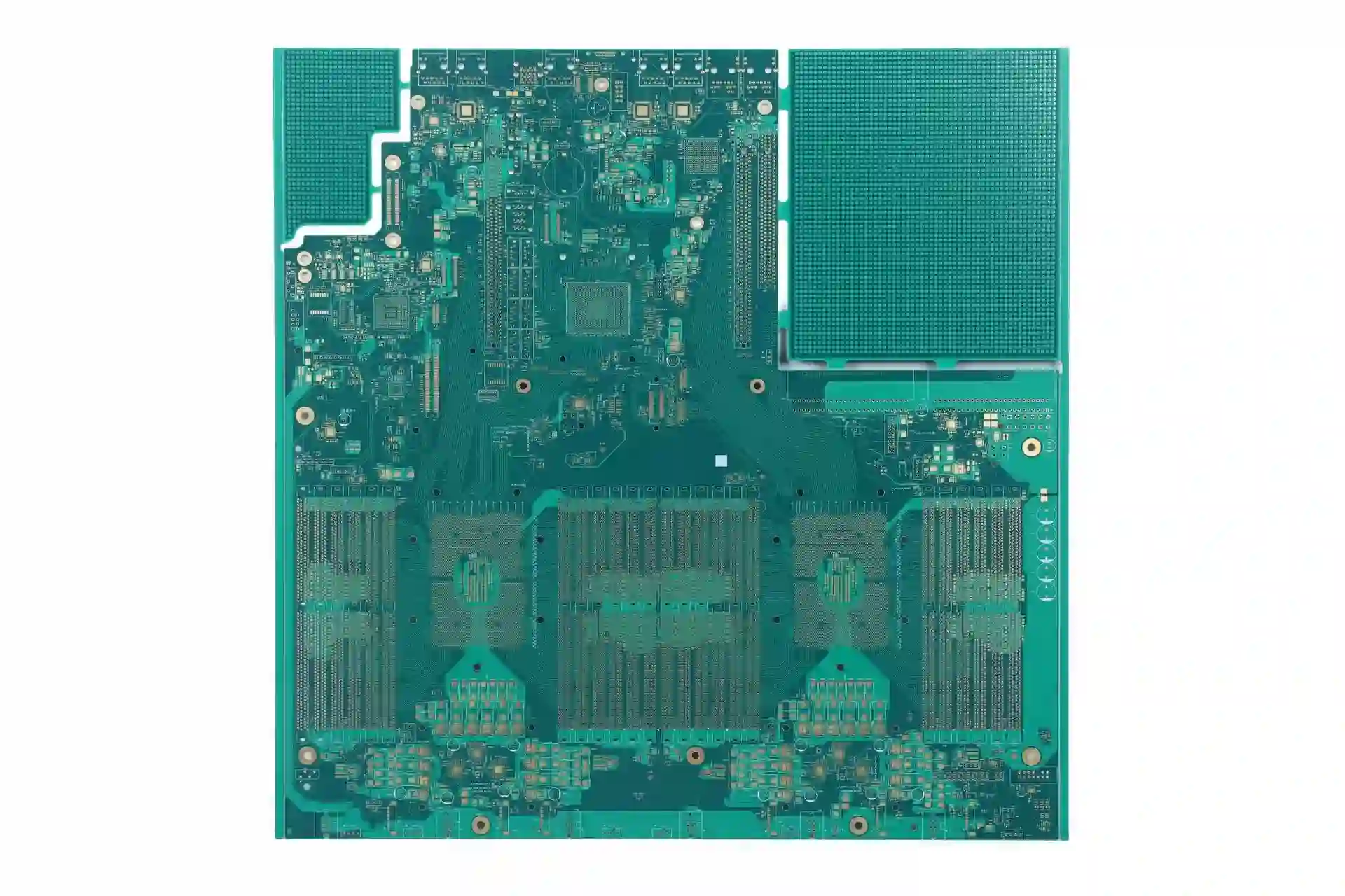
PCB Insider builds HDI PCBs for projects where ordinary multilayer fabrication runs out of routing room. We focus on the risk points that decide whether a high-density board works: 0.1mm laser microvias, 2/2 mil routing zones, sequential lamination, via-in-pad control, and assembly-ready DFM before the first article is released.
0.1mm
Laser microvia class
2/2 mil
Advanced trace/space
32 layers
Advanced PCB capacity
±5%
Impedance tolerance
HDI Is a Routing Decision, Not a Marketing Label
Printed circuit board density changes the manufacturing plan when through-hole vias, ordinary annular rings, and 4/4 mil routing consume too much space. HDI PCB manufacturing uses laser-drilled microvias, blind and buried structures, and sequential lamination to route compact electronics without making the board larger. The practical question is whether those process steps solve a real BGA, impedance, or size constraint; if not, standard multilayer fabrication is usually the better commercial choice.
Fine-Pitch BGA Escape Routing
HDI becomes practical when 0.4mm and 0.5mm BGA packages leave too little channel space for ordinary dog-bone vias.
0.1mm Laser Microvias
Laser microvias connect adjacent layers without consuming the routing space of through-hole vias.
Sequential Lamination Planning
Sequential lamination is powerful but expensive. We help buyers decide between 1+N+1, 2+N+2, staggered microvias, and stacked structures so the board gains.
2/2 Mil Routing by Review
Advanced HDI layouts may need 2/2 mil trace and spacing.
Via-in-Pad Decision Support
Via-in-pad helps dense BGAs, but filled and capped vias add cost and process risk.
Assembly-Ready HDI Output
HDI boards often move directly into SMT assembly with fine-pitch packages.
HDI PCB Capability Snapshot
Service focus
HDI PCB fabrication for compact, fine-pitch, high-density electronics
Layer count
1-8 layers standard, advanced builds up to 32 layers by review
Microvia class
0.1mm laser via capability from published PCB capabilities
Trace / space
4/4 mil standard, 2/2 mil advanced by design review
Via structures
Blind, buried, microvia, staggered, stacked, and via-in-pad by review
Lamination
Standard multilayer or sequential lamination for HDI stackups
Materials
FR-4, high-Tg FR-4, polyimide, Rogers, and application-specific laminates
Surface finishes
ENIG, OSP, HASL lead-free, immersion silver, immersion tin, hard gold
Impedance
±10% standard, ±5% advanced when stackup and materials are controlled
Testing
AOI, 100% electrical test, impedance test when specified, cross-section by request
Scope and Limits
Best fit
Fine-pitch BGA boards, compact medical modules, sensor electronics, high-speed embedded products, and multilayer designs where through-hole vias block.
Handled carefully
Stacked microvias, via-in-pad under dense packages, 2/2 mil routing, and ±5% impedance targets need complete data and engineering review before price.
Not the right fit
Simple two-layer or four-layer boards that route cleanly with 4/4 mil rules usually should stay with standard PCB manufacturing because HDI adds avoidable cost.
Hommer Zhao, Founder / Technical Expert
"The most expensive HDI mistake is choosing a stackup after the layout is already trapped. We review BGA fanout, microvia depth, and assembly impact before price, because those three details decide whether the board is manufacturable."
BGA Pitch Is the Fastest HDI Decision Filter
BGA pitch does not automatically prove that HDI is required, but it quickly exposes routing risk. Use the table below as an engineering conversation starter, then validate the result with the BGA Fanout Calculator and the Drill Aspect Ratio Calculator. HDI cost is justified when it removes routing layers, preserves impedance, or prevents package escape compromises that would hurt yield.
0.8mm BGA
Often standard multilayer
Dog-bone routing usually works when board area allows
0.65mm BGA
Borderline
May need tighter trace/space or added layers
0.5mm BGA
HDI review recommended
Fanout often benefits from microvias or via-in-pad
0.4mm BGA
HDI normally required
Laser microvias and via-in-pad are common
Stacked microvias
Use only when needed
Adds process risk; staggered may be safer when space allows
HDI Manufacturing Workflow
HDI projects fail when quoting treats the board like ordinary FR-4 fabrication. Our workflow makes the high-risk decisions visible before the first fabrication traveler is released.
Step 1
Fanout and stackup review
Engineering checks BGA pitch, ball count, layer assignment, microvia targets, and controlled impedance needs before quoting the HDI PCB build.
Step 2
DFM boundary setting
We separate standard areas from HDI-critical areas so 2/2 mil rules, filled vias, and tight registration are used where they affect routability.
Step 3
Sequential lamination planning
The stackup is reviewed for 1+N+1, 2+N+2, stacked, or staggered microvia strategy based on routing density, reliability, and cost trade-offs.
Step 4
Fabrication and inspection
Laser drilling, plating, imaging, lamination, AOI, electrical test, and optional impedance checks are aligned to the approved HDI manufacturing plan.
Step 5
Assembly handoff
Finished boards are reviewed for flatness, surface finish, panelization, fiducials, and via-in-pad notes before moving to SMT assembly or shipment.
Standards and Design References
HDI designs should be tied to named standards, not vague quality language. PCB Insider uses project requirements, IPC-aligned workmanship expectations, and buyer documentation to set inspection depth before production starts.
IPC Design Context
IPC-2226 covers high-density interconnect design concepts, while the broader IPC organization maintains electronics standards used across PCB manufacturing.
Microvia Risk Review
Microvia depth, aspect ratio, and stacking approach influence plating reliability, especially when sequential lamination cycles increase.
Impedance Control
High-speed HDI work should define material, dielectric thickness, copper weight, and tolerance before routing is frozen.
HDI PCB Manufacturing FAQ
When should I choose HDI PCB manufacturing instead of a standard multilayer PCB?
Choose HDI PCB manufacturing when the design cannot escape fine-pitch packages, high-speed nets, or compact routing with ordinary drilled vias. A common trigger is 0.5mm pitch BGA, dense connector breakout, or a board area target that forces 2/2 mil routing and 0.1mm laser microvias. Standard multilayer PCB fabrication is usually better when 4/4 mil routing and through-hole vias can meet the layout, because it avoids sequential lamination cost and schedule risk.
What HDI PCB files do you need for a manufacturing quote?
For an HDI PCB quote, send Gerber or ODB++ data, the intended stackup, drill tables, impedance targets, material notes, BGA pitch information, filled-via requirements, and assembly drawings. If via-in-pad is used, identify which vias need conductive or non-conductive fill and capping. A short note explaining the critical nets, controlled impedance layers, and target quantity helps engineering separate standard multilayer work from true HDI sequential lamination.
Can my 0.4mm or 0.5mm BGA design be built without HDI?
A 0.5mm BGA sometimes escapes with aggressive dog-bone routing, but 0.4mm BGA designs usually need HDI features such as via-in-pad, laser microvias, and tighter trace spacing. The practical decision depends on ball count, available routing channels, layer count, and whether power/ground balls block escape paths. PCB Insider reviews BGA fanout before quoting so buyers do not discover after layout release that the board needs a different stackup.
How does sequential lamination affect HDI PCB cost and lead time?
Sequential lamination adds cost and lead time because the fabricator builds, drills, plates, and presses the board in more than one manufacturing cycle. A 1+N+1 HDI board is usually simpler than a 2+N+2 or stacked microvia construction. The right stackup can reduce risk: staggered microvias often improve reliability compared with deep stacked structures, while unnecessary sequential cycles add price without helping routability.
I need 200 HDI PCBs for a medical device prototype. Is that too small?
A 200-piece HDI PCB prototype lot is a realistic fit when the design package is complete and the stackup is stable. Prototype HDI work still requires laser drilling, plating control, electrical test, and inspection, so the setup cost is higher than a simple FR-4 board. For medical electronics, buyers should define IPC class expectations, traceability needs, and assembly handoff requirements before quoting so the first article supports later validation work.
What quality checks are important for HDI PCB fabrication?
HDI PCB fabrication needs tighter verification than ordinary boards because microvias, fine traces, and via-in-pad structures hide failure modes. Important checks include DFM review, drill registration checks, AOI, 100% electrical test, impedance testing when specified, and cross-section review for high-risk microvia structures. IPC-2226 design guidance and IPC-6012 acceptance expectations are useful reference points when buyers define the quality plan.
Related Services
HDI fabrication usually sits between board design, bare-board manufacturing, and fine-pitch SMT assembly. Use these pages to choose the right manufacturing path.
PCB Manufacturing
Use this page for standard rigid, multilayer, flex, and broad fabrication programs.
Explore servicePCB Assembly
Move from HDI bare-board fabrication into SMT, BGA, and mixed-technology PCBA.
Explore service5G Antenna PCB
RF-aware antenna board fabrication when compact modules need HDI density plus controlled feed lines.
Explore serviceSMT Assembly
Dedicated surface mount assembly for the fine-pitch packages that often drive HDI.
Explore serviceGold Finger PCB Manufacturing
Hard-gold edge connector support when compact HDI cards plug into sockets or backplanes.
Explore serviceInstant PCB Quote
Send Gerber, ODB++, BOM, centroid, and HDI stackup notes for engineering review.
Explore serviceNeed an HDI PCB quote that checks the stackup first?
Send Gerber or ODB++ files, drill tables, BGA pitch, target quantity, and assembly notes. We'll review whether the design needs microvias, via-in-pad, sequential lamination, or a simpler multilayer path.