Rogers RO4350B PCB Guide: Datasheet, Properties & Design Considerations
Complete guide to Rogers RO4350B high-frequency PCB laminate. Learn about dielectric properties, design considerations, and applications for RF circuits.
Rogers RO4350B represents one of the most popular high-frequency circuit board laminates, engineered for performance-demanding wireless and radar applications from 500 MHz to 77 GHz. This ceramic-filled hydrocarbon composite offers electrical performance approaching PTFE materials while maintaining the processability of standard epoxy/glass laminates. This comprehensive guide covers RO4350B properties, design considerations, and applications for RF and microwave PCB designers.
Rogers RO4350B Overview
RO4350B is a proprietary woven glass-reinforced hydrocarbon/ceramic composite laminate developed by Rogers Corporation specifically for high-frequency and high data-rate PCB applications. The material achieves an optimal balance of electrical, thermal, and mechanical properties enabling precision RF circuit fabrication at reasonable cost.
Key attributes making RO4350B suitable for RF and microwave boards include:
- - Stable dielectric constant of 3.48 from 500MHz to 40GHz+
- Low loss tangent of 0.0037 minimizing signal attenuation
- Tight tolerances on εr and Dk for consistent performance
- Low Z-axis CTE for reliability through thermal cycling
- High thermal conductivity for power handling
- Lead-free compatible processing up to 260°C
- Excellent mechanical strength from glass reinforcement
- UL 94 V-0 flame rating for safety compliance
Unlike pure PTFE materials requiring special handling, RO4350B processes using standard FR-4 techniques including mechanical drilling, conventional etching, and standard multilayer lamination without sodium etching or unique handling procedures.
RO4350B Datasheet Parameters
Electrical Properties
| Parameter | Value | Test Condition | |-----------|-------|----------------| | Dielectric Constant (εr) | 3.48 | 10 GHz | | Loss Tangent | 0.0037 | 10 GHz | | Dissipation Factor | 0.0019 | 10 GHz | | Dielectric Tolerance | ±0.05 | - | | Dk Tolerance | ±0.002 | Up to 10 GHz | | Breakdown Voltage | 1.5 kV/mil | - | | Surface Resistivity | 1.5 × 10¹³ ohm | - | | Volume Resistivity | 1 × 10¹⁵ ohm-cm | - |
Thermal Properties
| Parameter | Value | |-----------|-------| | Z-Axis CTE | 32-41 ppm/°C | | XY CTE | 17 ppm/°C | | Glass Transition (Tg) | 280°C | | Decomposition (Td) | 340-390°C | | Thermal Conductivity | 0.69 W/m/K | | Lead-Free Process | 260°C Max |
Mechanical Properties
| Parameter | Value | |-----------|-------| | Moisture Absorption | <0.2% | | Copper Peel Strength | 1.3 lb/in | | Flexural Strength | High |
Dielectric Constant and Loss Tangent
Stable Dielectric Performance
The dielectric constant (Dk) indicates how much capacitance a material generates relative to air, directly affecting transmission line impedances and wavelengths. RO4350B provides a stable Dk of 3.48 from 500MHz to over 40GHz with minimal variation versus frequency.
This stability allows engineers to design controlled impedance transmission lines and matching networks working consistently across entire frequency ranges. Impedance calculations remain valid from low frequencies through millimeter-wave applications without frequency-dependent corrections.
Ultra-Low Loss Tangent
Loss tangent quantifies signal attenuation as RF energy propagates through the dielectric. RO4350B's loss tangent of 0.0037 ensures minimal signal loss, remaining under 0.004 up to 77GHz. For comparison, standard FR-4 has loss tangent around 0.02—roughly 5x higher than RO4350B.
Lower loss translates directly to better receiver sensitivity, higher transmitter efficiency, and improved signal-to-noise ratios in RF systems.
Tight Tolerances
Beyond stable Dk over frequency, RO4350B provides tight lot-to-lot dielectric constant tolerances of ±0.05. Panel-to-panel variance remains very consistent, making it easier for designers to account for material variations during layout.
Tighter εr tolerance provides more margin for meeting impedance targets, reducing the need for post-fabrication tuning or impedance trimming.
Thermal and Mechanical Properties
Low Z-Axis CTE
RO4350B exhibits low coefficient of thermal expansion along the z-axis (32-41 ppm/°C), providing reliability by minimizing dimensional changes during thermal cycling. High z-axis CTE causes copper cracking on inner signal layers, limiting board lifetimes.
RO4350B resists plating separations and electrical opens from excessive expansion and contraction, enabling reliable operation across wide temperature ranges.
Thermal Conductivity
With thermal conductivity of 0.69 W/m/K, RO4350B provides good heat spreading in dielectric layers preventing component hot spots. This helps maintain signal fidelity and component lifetime at high RF power levels where heat generation is significant.
Dimensional Stability
The woven glass fabric reinforcement provides excellent dimensional stability and flexural strength while maintaining low CTE and loss. The material resists microcracking and fracturing during fabrication and assembly handling.
XY CTE Matching
With XY CTE of 17 ppm/°C—close to copper's expansion rate—RO4350B maintains dimensional stability even at extreme temperatures. This prevents trace delamination and pad lifting during thermal cycling.
Material Grades and Variants
Rogers offers several RO4350B grades for different applications:
RO4350B High Reliability (HR): Mission-critical aerospace applications requiring maximum reliability and traceability.
RO4350B High Frequency (VF): Optimized for 77GHz mmWave designs and beyond, with tighter high-frequency specifications.
RO4350B Low Dk: Minimized loss tangent for applications prioritizing signal integrity.
RO4350B Bondply: Adhesiveless multilayer construction for complex stackups.
RT/duroid 5870: Lower cost variant for less demanding applications.
Consult material suppliers to determine optimal variants for specific RF performance, cost, and reliability requirements.
Design Considerations
Impedance Calculations
- - Use impedance calculators like Saturn PCB Toolkit or specialized RF tools
- Account for frequency-dependent Dk in models if operating across wide bandwidth
- Include pad and anti-pad shapes in calculations
- Allow for Dk and etch tolerances in impedance budgets
Layout Practices
- - Model discontinuities including stubs, vias, and bends
- Use teardrop pads on vias for improved reliability
- Minimize dielectrically exposed copper for lowest loss
- Limit glass weave skew to under 5 degrees
- Control trace width and spacing for consistent impedance
Manufacturing Considerations
- - Watch for resin starvation, voids, and thickness variations
- Standard FR-4 processing equipment works for RO4350B
- Mechanical drilling and conventional etching apply
- Standard multilayer lamination techniques work
- No special sodium etching required unlike pure PTFE
Mixed Dielectric Stackups
Combining RO4350B with FR-4 in hybrid stackups reduces costs 30-50% while maintaining RF performance where needed. Use RO4350B for RF signal layers and FR-4 for power distribution and low-frequency signals.
RO4350B Applications
Telecommunications
- - 5G NR base stations and infrastructure
- Cellular user equipment RF front-ends
- Wireless backhaul systems
- Small cell antenna systems
Automotive
- - 77GHz automotive radar sensors
- V2X communication modules
- Collision avoidance systems
- Autonomous driving sensors
Aerospace and Defense
- - Satellite communication systems
- Military radar systems
- Electronic warfare equipment
- Avionics communication systems
Test and Measurement
- - RF test fixtures and probes
- Spectrum analyzer components
- Network analyzer calibration standards
- Signal generators
Other Applications
- - High-speed data links and backplanes
- Medical diagnostic imaging equipment
- Industrial sensors and control systems
- GPS and navigation systems
Comparison with Alternative Laminates
| Parameter | RO4350B | RO4003C | FR-4 High-Tg | |-----------|---------|---------|---------------| | Dielectric Constant | 3.48 | 3.55 | 4.2-4.5 | | Loss Tangent | 0.0037 | 0.0027 | 0.02 | | Dk Tolerance | ±0.05 | ±0.079 | ±0.2 | | Z-Axis CTE | 41 ppm/°C | 60 ppm/°C | 60-70 ppm/°C | | Max Frequency | 77+ GHz | 40+ GHz | ~2 GHz | | Cost | Medium | Medium | Low | | Processing | Standard | Standard | Standard |
RO4350B provides excellent balance of performance and cost for most RF applications. RO4003C offers slightly lower loss for critical applications. FR-4 suffices only for frequencies below about 2GHz.
When to Use RO4350B vs FR-4
- Choose RO4350B for:
- Operating frequencies above 2GHz
- Tight impedance control (±5% or tighter)
- Temperature extremes (-50°C to +150°C)
- High-power RF requiring thermal management
- Low-loss signal transmission requirements
- Consistent performance across frequency range
- FR-4 may suffice for:
- Frequencies below 1-2GHz
- Non-critical impedance applications
- Cost-sensitive consumer products
- Digital circuits without high-speed signals
Cost Considerations
Rogers RO4350B costs typically range $200-$800 per square meter for raw material—significantly higher than FR-4 but lower than pure PTFE laminates. Finished board costs vary based on complexity, layer count, and volume.
Prototype quantities (10cm × 10cm, 5 pieces) start around $100-150, while production volumes offer 20-40% savings. Mixed dielectric stackups combining RO4350B with FR-4 reduce overall costs while maintaining RF performance.
Material Availability
Rogers partners with authorized distributors worldwide stocking various RO4350B configurations:
- - Dielectric thicknesses from 0.005" to 0.062"
- Prepregs with 106-211 glass styles
- Copper foil bonds from 0.5 to 3 oz
- Panel and cut sheet formats
- Quick-turn availability for prototypes
Work with PCB manufacturers to ensure consistent supply tailored to specific thickness and copper weight requirements.
Summary
Rogers RO4350B delivers an ideal microwave substrate solution for precision RF circuits up to 77GHz requiring stable dielectric properties and low loss. Its tight tolerances, high thermal conductivity, lead-free process capability, and standard processing compatibility make RO4350B a versatile high-frequency PCB material. Careful impedance modeling when designing on RO4350B ensures repeatable RF performance across fabricated boards.
For Rogers RO4350B PCB manufacturing and expert RF design support, contact WellPCB for competitive quotes and technical guidance.
Frequently Asked Questions
What frequencies can RO4350B support?
RO4350B provides stable dielectric performance from 500MHz to at least 40GHz, with the VF (high frequency) version extending capability to 77GHz and beyond. Loss tangent remains under 0.004 across this entire range.
Can RO4350B be processed like standard FR-4?
Yes, RO4350B uses standard FR-4 processing including mechanical drilling, conventional etching, and standard multilayer lamination. Unlike pure PTFE materials, no special sodium etching or unique handling procedures are required.
What is the z-axis CTE of RO4350B?
RO4350B has z-axis CTE of 32-41 ppm/°C depending on specific grade, minimizing dimensional changes through temperature excursions and avoiding reliability issues from thermal cycling.
Does RO4350B meet UL flammability requirements?
RO4350B achieves UL 94 V-0 rating for flame resistance, meeting safety requirements for consumer, industrial, and high-power electronics applications.
How does RO4350B compare to pure PTFE laminates?
RO4350B offers electrical performance approaching PTFE at lower cost and with standard FR-4 processing. Pure PTFE provides slightly lower loss but requires special handling and sodium etching that increases manufacturing complexity and cost.
Related Articles
Continue exploring similar topics
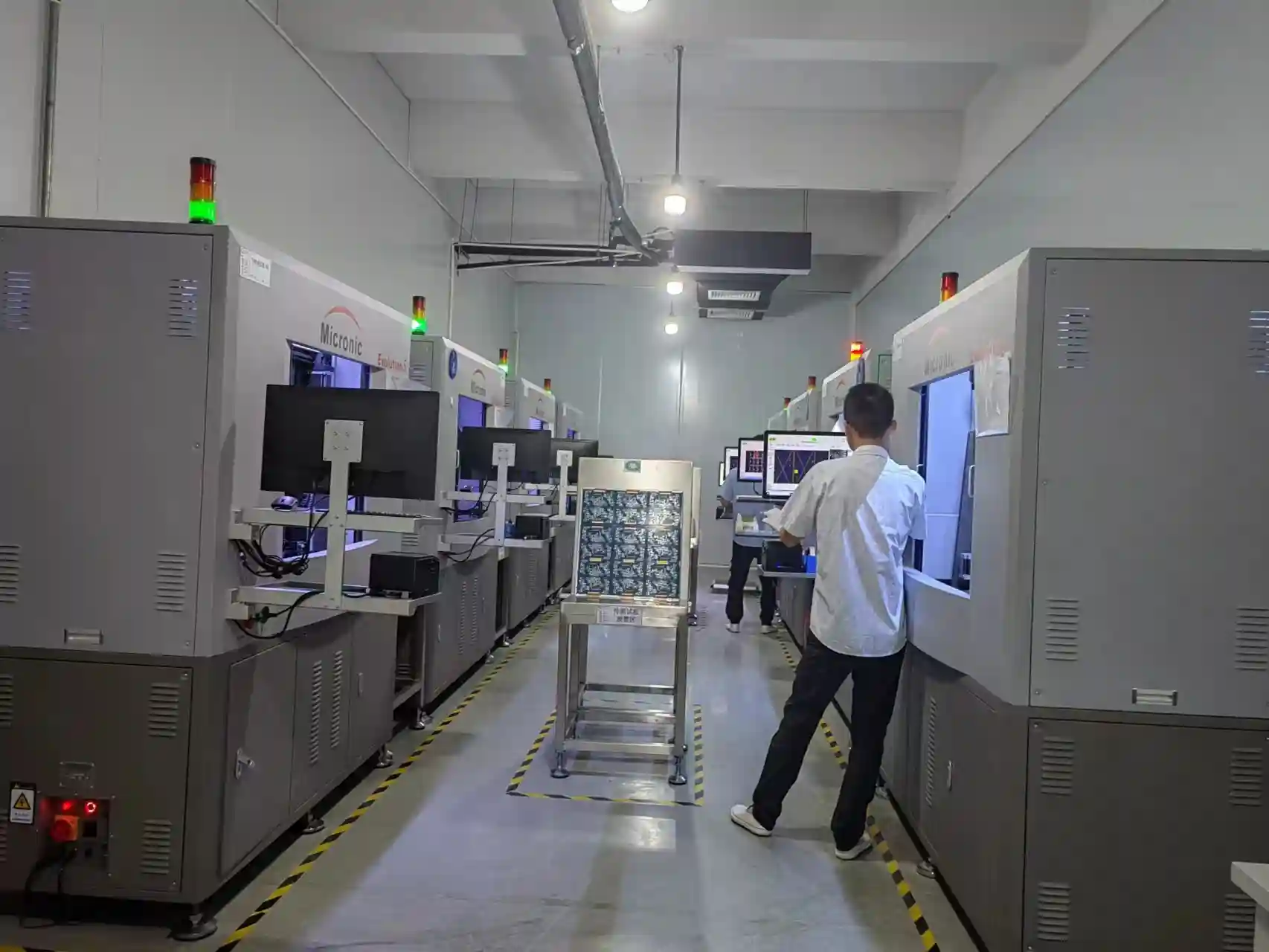
AOI Testing Guide: PCB Automated Optical Inspection Explained
Complete guide to Automated Optical Inspection (AOI) for PCB manufacturing. Learn how AOI works, defect detection capabilities, 2D vs 3D systems, and implementation best practices.
Bed of Nails Test Fixture Guide: PCB In-Circuit Testing Explained
Complete guide to bed of nails test fixtures for PCB testing. Learn about fixture types, pogo pins, ICT procedures, and quality control applications.
Double-Sided PCB: Complete Design and Manufacturing Guide
Master double-sided PCB design with our comprehensive guide covering manufacturing processes, layout strategies, via specifications, and cost optimization tips.
Ready to bring your PCB design to life?
Get an instant quote for your custom PCB fabrication and assembly needs.
Get Instant Quote