AOI Testing Guide: PCB Automated Optical Inspection Explained
Complete guide to Automated Optical Inspection (AOI) for PCB manufacturing. Learn how AOI works, defect detection capabilities, 2D vs 3D systems, and implementation best practices.
Automated Optical Inspection represents one of the most significant advancements in PCB quality control over the past two decades. As electronic assemblies become increasingly miniaturized and component densities continue to rise, the human eye simply cannot keep pace with inspection demands. AOI technology fills this gap by providing rapid, consistent, and highly accurate visual examination of circuit boards at speeds that would be impossible for manual inspection teams to achieve.
The fundamental principle behind AOI is deceptively simple: high-resolution cameras capture detailed images of a circuit board, and sophisticated software algorithms compare these images against known-good references to identify anomalies. However, the engineering required to make this process reliable at production speeds involves complex interactions between lighting systems, optical components, image processing algorithms, and defect classification logic. Understanding how these elements work together is essential for anyone involved in electronics manufacturing quality assurance.
The Mechanics of Automated Optical Inspection
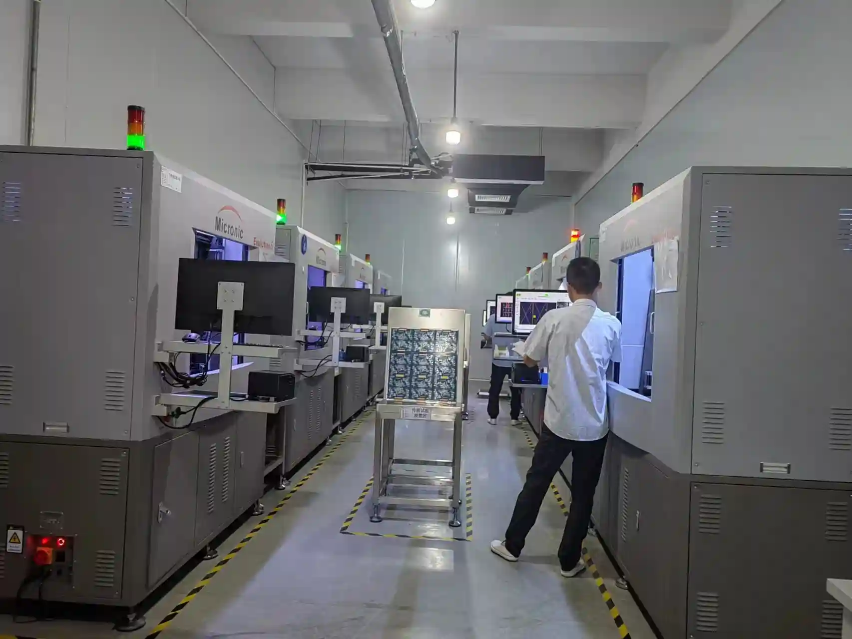
AOI systems operate through a carefully orchestrated sequence of image acquisition and analysis. When a circuit board enters the inspection zone, multiple high-resolution cameras positioned at various angles capture overlapping images that cover the entire board surface. The lighting configuration plays a crucial role in this process, with LED arrays providing illumination from different angles to reveal surface features that might otherwise remain hidden. Some systems employ colored lighting or ultraviolet illumination to enhance contrast for specific defect types.
The captured images undergo preprocessing to correct for variations in lighting intensity and camera lens distortion. Once normalized, the software compares each region of the board against reference data, which may come from a previously inspected "golden board" or from CAD design files. Advanced systems use pattern matching algorithms that can identify components regardless of minor variations in their appearance, while simultaneously checking that each component is present, correctly positioned, and properly oriented.
Image analysis algorithms examine multiple characteristics simultaneously. The software measures component positions relative to their nominal pad locations, typically achieving accuracy within 5 to 10 micrometers per pixel for fine-pitch components. Color analysis helps distinguish between different component types and identifies marking anomalies. Shape recognition algorithms verify that components match their expected outlines, flagging any that appear damaged, missing, or incorrectly placed.
Defect Categories Detected Through AOI
The range of defects that AOI systems can identify spans nearly every aspect of PCB assembly quality. Component-level defects represent the most common category, including missing parts that were never placed, shifted components that landed off-center from their pads, wrong components installed in place of the specified parts, and tombstoned chips where one end lifted during reflow soldering. Modern AOI systems achieve detection rates exceeding 99% for these visible placement errors.
Solder joint inspection presents greater challenges because joint quality depends on three-dimensional characteristics that may not be fully visible from above. Nevertheless, AOI effectively identifies solder bridges where excess solder creates unintended connections between adjacent pads, insufficient solder that fails to wet properly onto component leads, solder balls that have splattered across the board surface, and lifted leads where component terminations have separated from their pads. The transition to 3D AOI has significantly improved detection rates for solder-related defects.
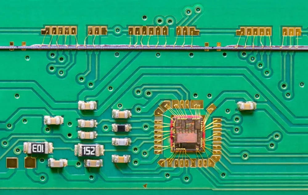
PCB substrate defects fall within AOI's detection capabilities as well. Scratched or damaged traces, contamination from foreign particles, lifted pads, and copper exposure from damaged solder mask all appear in inspection results. For bare board inspection before assembly, AOI verifies that conductor traces match design specifications, identifying narrowed traces that might cause reliability issues even if they remain electrically continuous. This capability proves especially valuable for high-frequency applications where trace geometry directly affects signal integrity.
Understanding 2D Versus 3D AOI Technology
Traditional 2D AOI systems capture flat images from a single overhead perspective, relying on lighting variations and shadow analysis to infer height information. While these systems remain effective for many applications, they struggle with certain defect types that depend on three-dimensional characteristics. A solder joint might appear acceptable in a top-down view while actually containing insufficient solder volume or excessive voiding that only becomes apparent when examined from multiple angles.
3D AOI technology addresses these limitations by constructing actual three-dimensional models of the inspected surface. Multiple cameras positioned at different angles capture images simultaneously, and triangulation algorithms calculate precise height values for every point on the board. Some systems project structured light patterns onto the surface to enhance depth measurement accuracy. The resulting 3D model reveals solder joint shapes, component heights, and surface features with measurement precision typically within a few micrometers.
The advantages of 3D inspection extend beyond improved defect detection. Height measurement capabilities enable accurate solder volume calculations, allowing manufacturers to identify joints that have too little solder to ensure long-term reliability or too much solder that might cause bridging during thermal cycling. Component coplanarity measurements verify that parts sit flat against the board surface, catching lifted leads or warped packages that could create intermittent connections. For manufacturers dealing with fine-pitch components or high-reliability applications, 3D AOI has become essentially mandatory.
The AOI Inspection Process Flow
Implementing AOI effectively requires careful attention to the complete inspection workflow, beginning with system programming and extending through production operation and result analysis. The programming phase establishes the reference data and detection parameters that determine inspection performance. Skilled technicians must balance detection sensitivity against false call rates, setting thresholds tight enough to catch genuine defects while loose enough to accept normal manufacturing variations.
Two primary programming approaches exist for creating inspection references. The golden board method involves scanning a known-good assembly to create a reference template. The system learns acceptable appearances by examining multiple examples of properly built boards, gradually building tolerance windows that accommodate normal variation. Alternatively, CAD-based programming imports design data directly, generating component models and placement specifications from the original design files. This approach eliminates the need for physical reference boards and ensures that inspection criteria match design intent precisely.
During production, boards enter the AOI system through automated handling equipment that positions each assembly precisely within the camera field of view. The inspection cycle typically requires between 10 and 60 seconds depending on board size and inspection thoroughness. Detected anomalies trigger real-time alerts, and failed boards route to repair stations where technicians can examine flagged defects and determine appropriate corrective actions. Statistical process control data feeds back into manufacturing systems to identify trends before they result in quality escapes.
Calibration and Maintenance Requirements
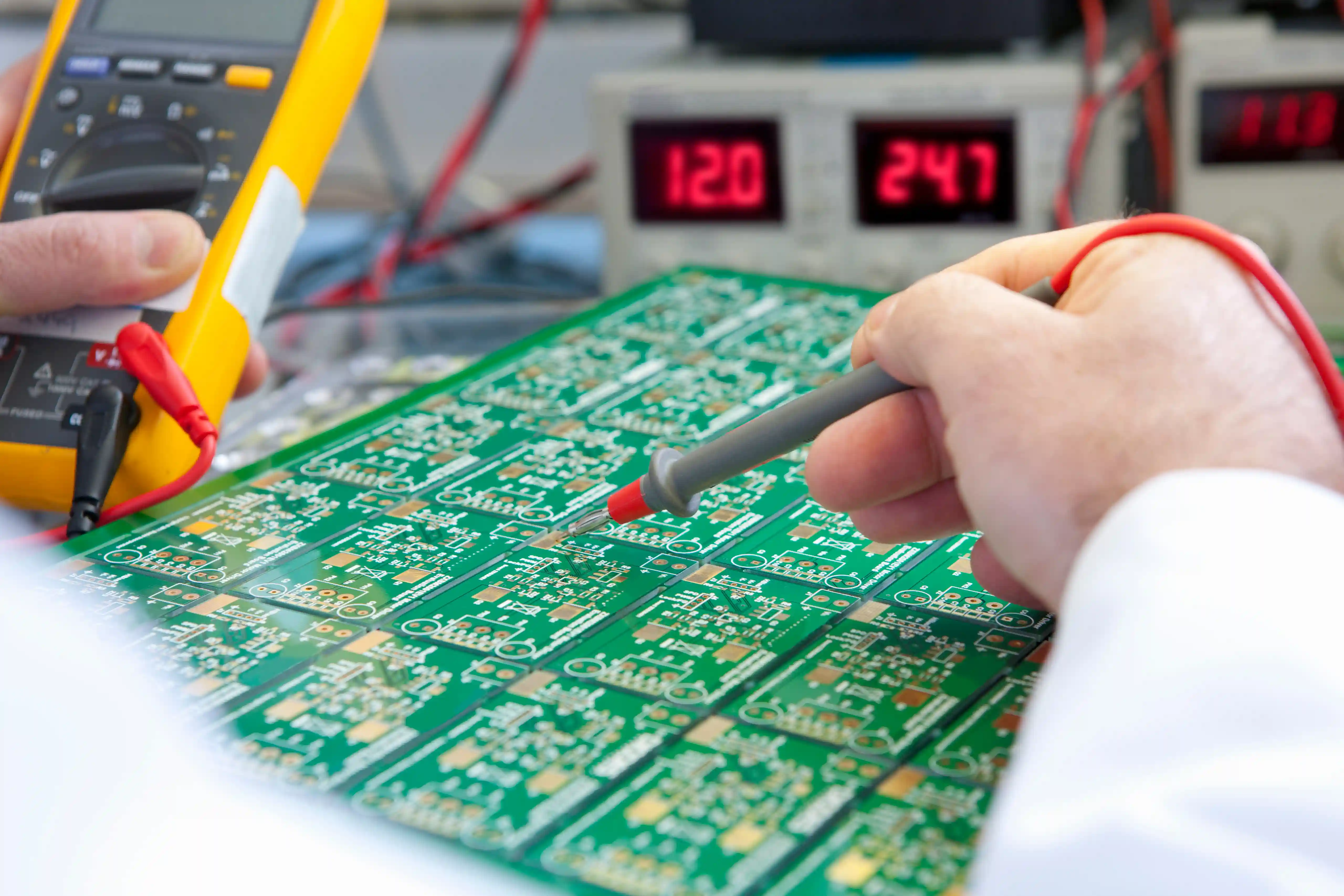
AOI system accuracy depends on regular calibration and preventive maintenance. Camera focus, lighting intensity, and conveyor positioning must remain within specified tolerances to ensure consistent inspection results. Most manufacturers establish calibration schedules ranging from weekly verification checks to comprehensive monthly or quarterly calibrations depending on production volume and quality requirements.
Environmental factors can significantly impact inspection performance. Temperature variations cause camera lenses to shift focus slightly, affecting measurement accuracy. Vibration from nearby equipment may blur images or cause registration errors. Dust accumulation on lenses or lighting fixtures degrades image quality gradually over time. Facilities operating AOI equipment should maintain stable temperature and humidity levels while implementing regular cleaning procedures.
Calibration verification typically involves scanning standard test targets with known dimensions and defect patterns. These targets contain features that exercise the full range of system capabilities, from fine-pitch component detection to solder joint analysis. Measurements must fall within specified tolerances, and detection algorithms must correctly identify all intentional defects without flagging acceptable features. When results drift outside acceptable ranges, technicians perform adjustments or escalate to equipment vendors for service.
Comparing AOI With Alternative Inspection Methods
No single inspection technology can detect every possible defect type, making it essential to understand how AOI complements other quality verification methods. In-circuit testing uses electrical probes to verify circuit functionality, catching defects that produce electrical failures regardless of their visual appearance. However, ICT cannot identify problems that might cause failures later, such as marginal solder joints that remain functional initially but degrade over time. AOI excels at finding these visual indicators of potential reliability issues.
X-ray inspection provides visibility beneath opaque components where optical methods cannot see. Ball grid array packages, for instance, have their solder connections completely hidden under the component body. Only X-ray imaging can reveal whether these joints formed properly, identifying voids, bridges, or insufficient solder that AOI would miss entirely. The combination of AOI for surface inspection and X-ray for hidden joints provides comprehensive coverage for complex assemblies.
Solder paste inspection occurs earlier in the assembly process, examining paste deposits after stencil printing but before component placement. SPI systems measure paste volume, height, and position, identifying printing defects before they become assembly defects. Since the majority of solder joint problems originate from printing issues, SPI provides early warning that allows correction before defective boards progress through the assembly line. Many manufacturers integrate SPI, AOI, and X-ray inspection into a coordinated quality system where each technology handles the defect types it detects most effectively.
Limitations and Challenges of AOI Technology
Despite its capabilities, AOI technology has inherent limitations that manufacturers must understand and accommodate. The most fundamental constraint is that AOI can only detect defects it has been programmed to recognize. Novel defect types or unusual failure modes may escape detection until technicians update the inspection program to address them. This limitation underscores the importance of continuous program refinement based on field feedback and failure analysis results.
False calls remain a persistent challenge for AOI implementations. When the system incorrectly flags acceptable boards as defective, operators must spend time verifying each call, reducing throughput and potentially causing good product to be scrapped. Conversely, detection thresholds set too loosely may allow genuine defects to escape into finished goods. Finding the optimal balance requires ongoing effort, and even well-tuned systems typically generate some percentage of false calls that operators must review.
Certain defect types remain difficult or impossible for AOI to detect reliably. Subsurface defects within the PCB laminate, such as delamination or internal cracks, cannot be seen optically. Cold solder joints may appear visually acceptable while lacking the metallurgical bond necessary for reliable electrical connection. Intermittent defects that only manifest under certain conditions obviously cannot be detected through static visual inspection. Recognizing these blind spots helps manufacturers deploy complementary inspection methods appropriately.
Best Practices for AOI Implementation
Successful AOI deployment begins with selecting equipment matched to production requirements. High-speed inline systems provide the throughput needed for volume manufacturing, inspecting boards immediately after SMT placement while the production line continues operating. Standalone systems offer flexibility for lower-volume operations or quality verification sampling. The choice depends on production volumes, product mix, and quality objectives specific to each manufacturing environment.
Program development represents the most critical success factor for AOI effectiveness. Rushed or incomplete programming leads to excessive false calls and missed defects. Skilled programmers should analyze each assembly design to identify inspection challenges, develop appropriate algorithms and thresholds for each component and solder joint type, and validate detection performance using known defective samples. Investing adequate time in program development pays dividends through improved detection rates and reduced false call rates during production.
Integrating AOI data with broader manufacturing intelligence systems multiplies its value beyond simple pass/fail decisions. Tracking defect trends over time reveals process drift before it causes quality problems. Correlating AOI findings with SPI data identifies relationships between paste printing variations and solder joint defects. Analyzing defect patterns by component type, placement position, or time of day uncovers root causes that might otherwise remain hidden. This analytical approach transforms AOI from a simple inspection gate into a powerful process improvement tool.
Industry Applications and Requirements
Different industry sectors impose varying requirements on AOI inspection stringency. Automotive electronics demand zero-defect quality due to safety implications and the extreme cost of field failures. Medical device manufacturers face regulatory requirements for documented inspection processes and complete traceability. Aerospace and defense applications often specify 100% inspection with enhanced screening for mission-critical assemblies.
Consumer electronics manufacturing prioritizes throughput and cost efficiency while maintaining acceptable quality levels. High-speed AOI systems capable of inspecting boards in under 15 seconds enable these manufacturers to achieve production targets without sacrificing inspection coverage. The balance between speed and thoroughness requires careful optimization based on defect risk analysis and quality cost tradeoffs.
Emerging applications in areas like electric vehicle power electronics and 5G telecommunications infrastructure create new AOI challenges. These products often combine high-power components with sensitive RF circuits on densely populated boards. Power semiconductor inspection requires detection of anomalies that might cause thermal management problems under load. RF circuit inspection must verify precise component placement that affects signal performance. AOI systems continue evolving to address these specialized requirements.
Conclusion
Automated Optical Inspection has become indispensable for modern PCB manufacturing, providing the rapid, accurate, and consistent inspection that complex electronic assemblies require. From detecting missing components and placement errors to identifying solder joint defects and substrate anomalies, AOI catches problems that would be impossible to find through manual inspection alone. The evolution from 2D to 3D systems has expanded detection capabilities further, enabling accurate height measurements and solder volume analysis that enhance quality assurance for fine-pitch and high-reliability applications.
Effective AOI implementation requires understanding both the technology's capabilities and its limitations. Careful program development, regular calibration, and integration with complementary inspection methods maximize detection effectiveness while minimizing false calls. When deployed as part of a comprehensive quality management system, AOI provides the visibility needed to identify process issues early, reduce defect escape rates, and achieve the consistent quality that today's electronic products demand.
For professional PCB manufacturing and assembly services with comprehensive AOI inspection, contact WellPCB for a quote tailored to your specific quality requirements.
Frequently Asked Questions
What defects can AOI detect that manual inspection might miss?
AOI excels at detecting subtle defects that human inspectors often overlook due to fatigue or the limitations of visual acuity. These include slightly shifted components that remain within pad boundaries but exceed placement tolerances, minor solder bridges between fine-pitch pins, small foreign particles on the board surface, and gradual trends in placement accuracy that indicate equipment drift. The consistency of automated inspection eliminates the variability inherent in manual processes.
How does 3D AOI improve detection compared to 2D systems?
Three-dimensional inspection provides actual height measurements rather than inferring depth from shadows and lighting variations. This enables accurate solder volume calculations to identify joints with too little or too much solder, coplanarity measurements to detect lifted component leads, and precise shape analysis of solder fillet profiles. For fine-pitch components and BGA periphery joints, 3D measurement substantially improves defect detection rates.
Can AOI completely replace other inspection methods?
No, AOI complements rather than replaces other quality verification methods. Electrical testing verifies circuit functionality that cannot be determined visually. X-ray inspection reveals defects beneath opaque components like BGAs. Solder paste inspection catches printing defects before assembly. A comprehensive quality strategy uses multiple inspection technologies, each addressing the defect types it detects most effectively.
What factors affect AOI false call rates?
Programming quality has the greatest impact on false call rates. Inspection parameters set too tightly flag normal manufacturing variations as defects. Inadequate training samples cause the system to reject acceptable appearance variations. Component database inaccuracies lead to misidentification. Environmental factors like lighting changes and temperature variations also contribute. Regular program refinement based on false call analysis gradually improves performance over time.
How long does it take to program AOI for a new product?
Programming time varies significantly based on board complexity. Simple assemblies with standard components might require only a few hours of programming effort. Complex boards with hundreds of unique components, fine-pitch devices, and mixed technology can require several days of programming and verification. CAD-based programming generally proceeds faster than golden board methods but still requires manual refinement for optimal results.
Related Articles
Continue exploring similar topics
Bed of Nails Test Fixture Guide: PCB In-Circuit Testing Explained
Complete guide to bed of nails test fixtures for PCB testing. Learn about fixture types, pogo pins, ICT procedures, and quality control applications.
Double-Sided PCB: Complete Design and Manufacturing Guide
Master double-sided PCB design with our comprehensive guide covering manufacturing processes, layout strategies, via specifications, and cost optimization tips.
Electronics Manufacturing Services (EMS): Complete Outsourcing Guide
Comprehensive guide to EMS providers covering outsourcing benefits, selection criteria, service offerings, and industry trends for 2025.
Ready to bring your PCB design to life?
Get an instant quote for your custom PCB fabrication and assembly needs.
Get Instant Quote