Double-Sided PCB: Complete Design and Manufacturing Guide
Master double-sided PCB design with our comprehensive guide covering manufacturing processes, layout strategies, via specifications, and cost optimization tips.
Double-sided printed circuit boards represent the most widely used PCB type in commercial electronics, striking an optimal balance between capability and cost. With copper traces on both surfaces connected through plated through-holes, these boards enable moderately complex circuits while remaining more economical than multilayer alternatives. This comprehensive guide covers everything from fundamental concepts to advanced design strategies for double-sided PCBs.
What is a Double-Sided PCB?
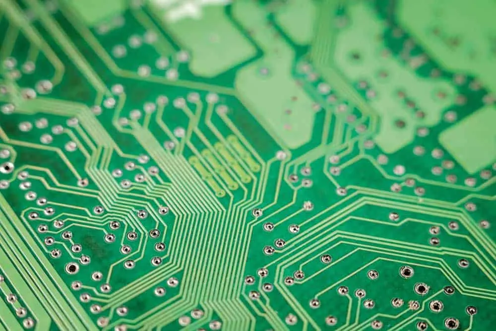
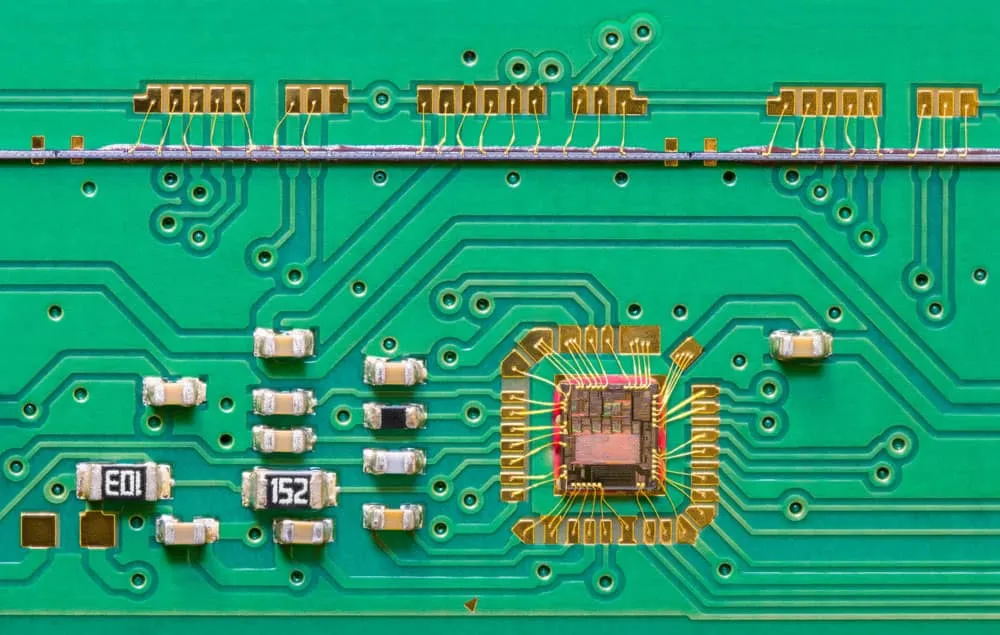
A double-sided PCB (also called 2-layer PCB) features copper conductors on both the top and bottom surfaces of an insulating substrate, typically FR-4 fiberglass. An insulating core separates the two copper layers, while plated through-holes (PTHs) called vias provide electrical connections between surfaces. This construction effectively doubles the available routing area compared to single-sided boards.
The ability to route traces on both surfaces dramatically increases layout flexibility. Signals that would require complex routing paths on a single layer can simply transition to the opposite side through a via, crossing other traces without interference. This capability makes double-sided PCBs suitable for circuits far more complex than single-sided boards can accommodate.
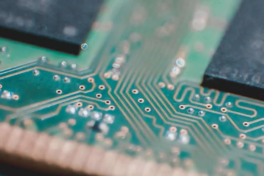
Vias form the critical bridges connecting the two copper layers. These small holes are drilled through the board and electroplated with copper to create reliable electrical connections. The quality of plated through-holes directly impacts PCB reliability, making PTH processing one of the most critical manufacturing steps. Modern mechanical drilling can achieve hole diameters down to 0.2mm, though 0.3mm remains the standard for cost-effective production.
Double-Sided vs Single-Sided PCB Comparison
Structural Differences
Single-sided boards feature copper on only one surface with components typically mounted on the opposite side. All routing must occur on the single copper layer, with crossovers impossible without jumper wires. Holes serve only for component mounting without electrical connection between layers.
Double-sided boards provide copper on both surfaces connected through plated vias. Components can mount on either or both sides, and traces can transition between layers as needed. This fundamental difference enables significantly more complex circuits within the same board area.
Routing Capability
Single-sided routing imposes severe constraints on circuit complexity. Traces cannot cross each other, forcing longer routing paths and limiting practical component density. Many circuits simply cannot be routed on a single layer without external jumper wires.
Double-sided routing eliminates crossing constraints through layer transitions. When one trace needs to cross another, it simply drops to the opposite layer through a via. This capability dramatically reduces board size for equivalent circuits and enables complexity levels impossible on single-layer boards.
Cost Considerations
Single-sided boards cost less to manufacture due to simpler processing without PTH plating requirements. However, the larger board sizes often required and design constraints may offset manufacturing savings. Single-sided construction suits only the simplest circuits.
Double-sided boards cost more per square inch but enable smaller designs and greater circuit density. For most applications, the capability improvements justify the modest cost premium. Double-sided construction has become the default for commercial electronics.
Manufacturing Complexity
Single-sided production follows relatively simple processes: imaging, etching, drilling (for mounting holes only), solder mask, and surface finish application. No plating operations are required.
Double-sided production requires additional plating processes to create conductive via connections. Electroless copper deposition followed by electrolytic copper plating builds up the PTH metallization. These additional steps increase manufacturing time and cost but enable the interconnection capability that makes double-sided boards practical.
Manufacturing Process Flow
Standard HASL/Immersion Gold Process
The typical double-sided PCB manufacturing sequence proceeds through these major steps:
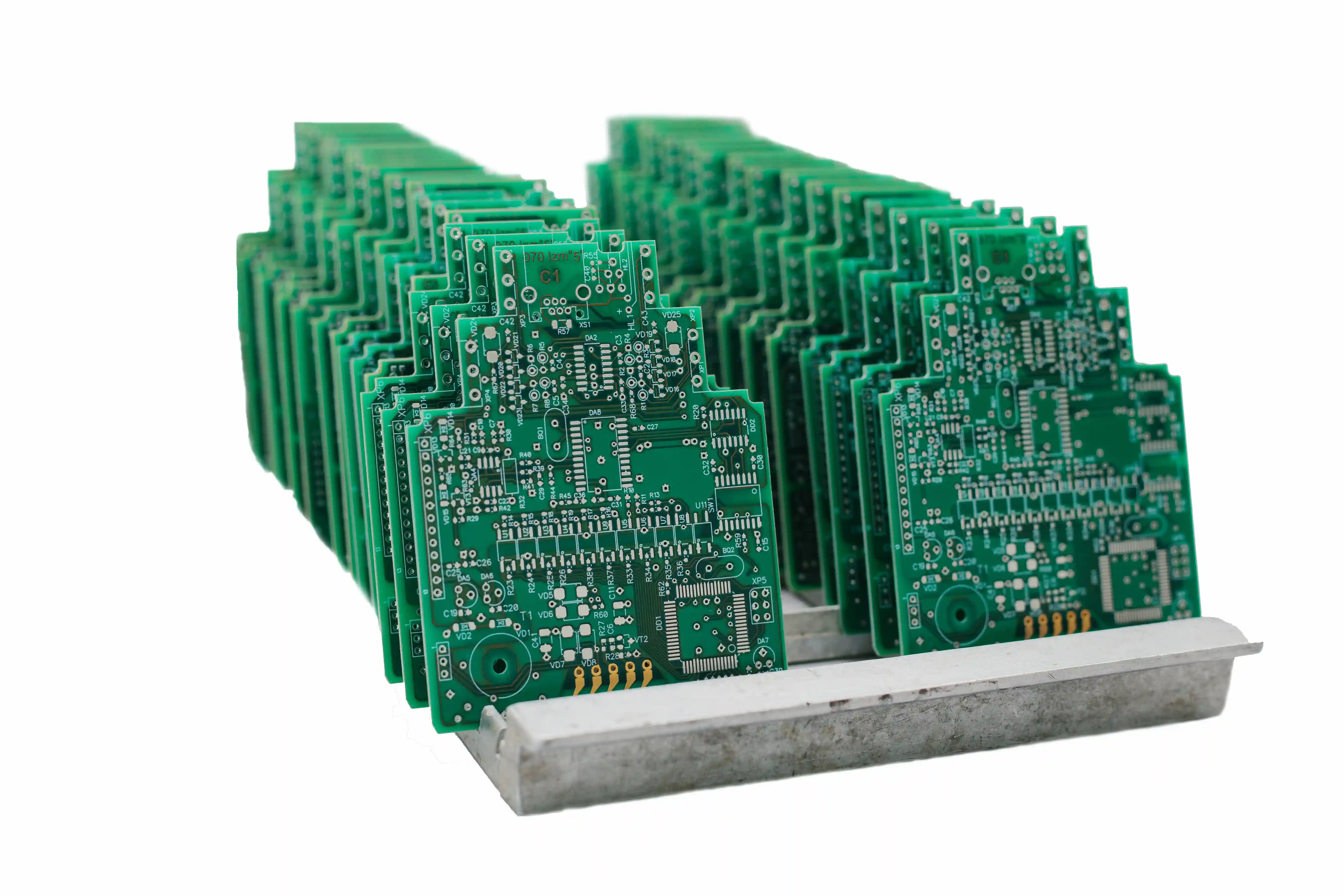
Material Preparation: Production begins with cutting copper-clad laminate (typically FR-4) to appropriate panel sizes. Standard laminate features copper foil bonded to both sides of the fiberglass core.
Drilling: CNC drilling machines create all through-holes including vias, component holes, and mounting holes. Drill bit selection and backing materials significantly impact hole quality. Proper dust collection prevents debris from contaminating subsequent processes.
Electroless Copper Deposition: After cleaning, the drilled panels undergo electroless copper plating. This chemical process deposits a thin copper layer on the non-conductive hole walls, making them conductive for subsequent electroplating. This step is crucial for reliable PTH formation.
Pattern Electroplating: Photoresist is applied and exposed through artwork masks to define the circuit pattern. Exposed areas are then electroplated to build up copper thickness on traces and in holes. Some processes plate the entire panel first, then define patterns.
Etching: Unplated copper is etched away, leaving only the desired circuit patterns. The plated traces and through-holes resist the etching solution, defining the final conductor geometry.
Solder Mask Application: Liquid photoimageable solder mask covers the board surface, protecting copper and defining solder pad openings. The mask is exposed and developed to create precise pad apertures.
Surface Finish: HASL (Hot Air Solder Leveling), ENIG (Electroless Nickel Immersion Gold), OSP, or other finishes are applied to protect exposed copper pads and enhance solderability.
Silkscreen Printing: Component reference designators, polarity indicators, and other markings are printed on the solder mask surface.
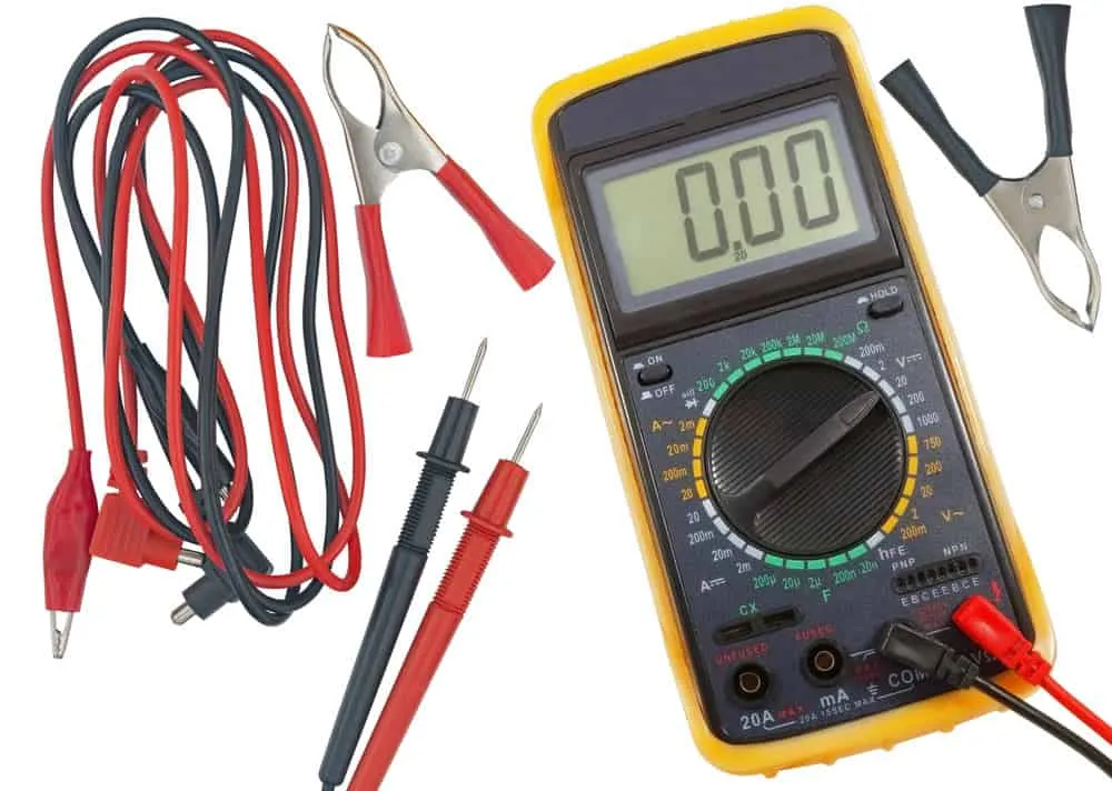
Final Fabrication: Routing or V-scoring separates individual boards from panels. Electrical testing (flying probe or fixture-based) verifies connectivity before packaging and shipment.
PTH Formation Details
Plated through-hole quality critically impacts PCB reliability. The metallization process involves precise chemistry and timing to ensure adequate copper thickness and adhesion on hole walls.
Electroless copper works through catalytic reduction reactions. After activating hole walls with palladium-based catalysts, copper ions in solution reduce to metallic copper on the catalyzed surfaces. This thin copper layer (typically 0.5-1.0 microns) provides the conductive base for subsequent electroplating.
Electrolytic copper plating builds the copper thickness to specification, typically 25 microns minimum in the holes. The electroplating bath composition, current density, and agitation all affect deposit quality. Proper throwing power ensures adequate plating even in small diameter holes.
Environmental concerns have driven development of alternative PTH technologies. Black hole (carbon-based), direct metallization, and conductive polymer processes reduce chemical waste compared to traditional electroless copper while maintaining reliability.
Design Guidelines and Best Practices
Trace Width and Spacing
Standard manufacturing typically supports 6 mil (0.15mm) minimum trace width and spacing. This specification provides good yield and reasonable cost for most applications. Designs requiring 4 mil features increase manufacturing difficulty and cost by 25-40%.
Power traces require width calculations based on current requirements. For 1oz copper at 1A current, minimum trace width of 20 mils prevents excessive heating. Higher currents or elevated ambient temperatures require proportionally wider traces. Online calculators simplify these calculations.
High-voltage isolation requires increased spacing beyond minimum manufacturing capability. IPC-2221 provides guidelines based on voltage levels and coating status. Always verify spacing requirements for your specific application.
Ground Plane Strategy
Double-sided designs benefit significantly from dedicating one layer primarily to ground plane. The recommended approach uses the top layer for signal routing and power distribution while maintaining a continuous ground plane on the bottom layer.
Minimize cuts and splits in the ground plane. Routing signals through the ground layer creates slots that interrupt return current paths, increasing noise and EMI. When signals must route on the ground layer, keep traces short and avoid cutting across sensitive areas.
Place ground vias liberally throughout the board. Stitching vias connect ground areas and provide short return current paths for signals transitioning between layers. Position ground vias within 0.5mm of signal vias to minimize return loop inductance.
Via Specifications
Standard vias use 0.3mm drill diameter with 0.6mm finished pad diameter, providing 0.15mm annular ring. This specification works reliably with mechanical drilling and standard manufacturing processes. Smaller vias (0.2mm) require laser drilling at significantly higher cost.
Annular ring refers to the copper remaining around the drilled hole. Minimum 5 mil (0.127mm) annular ring maintains reliable connections. Larger rings improve yield, particularly for through-hole component pads where mechanical stress occurs during soldering.
- Via placement guidelines include:
- Maintain minimum 0.5mm via-to-via spacing
- Keep minimum 0.3mm via-to-pad clearance
- Place ground vias near signal vias for return current paths
- Use thermal relief patterns on vias connecting to copper pours
- Consider via tenting to prevent solder wicking during assembly
Component Placement
Position connectors at board edges for external access. Group related components together to minimize trace lengths. Place decoupling capacitors within 5mm of IC power pins for effective high-frequency bypassing.
Keep heat-generating components spaced appropriately and away from temperature-sensitive devices. Provide adequate clearance around mounting holes. Position test points for probe access during debugging and production testing.
For double-sided assembly, consider which components mount on each side. Heavier components typically go on the primary side to prevent falling during reflow of the secondary side. Temperature-sensitive components may need placement on the secondary side to minimize thermal exposure.
Common Design Mistakes to Avoid
Ground Plane Splitting
Routing signal traces through the ground plane creates slots that interrupt return current flow. This forces return currents to take longer paths around the slots, increasing loop inductance and radiated emissions. Keep the ground layer as continuous as possible.
Undersized Power Traces
Using narrow traces (6-10 mil) for power distribution causes voltage drops and local heating. Calculate appropriate trace widths based on current requirements. For 1A with 1oz copper, use minimum 20 mil width. Higher currents require proportionally wider traces or copper pours.
Poor Decoupling Capacitor Placement
Positioning decoupling capacitors far from IC power pins reduces their effectiveness. High-frequency noise filtering requires short, low-inductance connections. Place 0.1µF ceramic capacitors within 5mm of each IC power pin with direct traces to both power and ground.
Missing Ground Vias Near Signal Vias
Signal vias without nearby ground vias create large return current loops, increasing noise susceptibility and emissions. Place a ground via within 0.5mm of every signal via that transitions between layers.
Excessive Via Usage
While vias enable routing flexibility, excessive use without purpose can create problems. Each via adds parasitic inductance and consumes board space. Use vias strategically rather than placing them arbitrarily throughout the design.
Assembly Considerations

Double-Sided Reflow Process
Double-sided SMT assembly requires two reflow passes. The first side receives solder paste, components, and reflow soldering. The board then flips for the second side to receive the same treatment.
During the second reflow pass, components on the first side experience another thermal cycle. Smaller components typically survive due to surface tension holding them in place even when solder remelts. Heavier components risk falling if they exceed the solder surface tension capability.
Component Placement Strategy
Place smaller, lighter components on the first side (which goes through reflow twice). Heavier components and those with many leads (larger BGAs, heavy connectors) go on the second side to minimize fall-off risk.
Temperature-sensitive components should be placed on the second side to minimize thermal exposure. Verify that all components can withstand at least two reflow cycles (three if rework might be needed).
For BGA placement, consider that first-side mounting subjects the BGA to two reflows, potentially affecting joint quality. However, second-side mounting occurs after the board has experienced thermal stress, potentially causing warpage that affects alignment. Prioritize minimizing board warpage through proper design and process control.
Soldering Best Practices
For manual soldering of through-hole components on double-sided boards, ensure via connections are properly wetted. The solder should flow through the via to appear on both sides, confirming reliable connection. Cut protruding leads flush to prevent interference with adjacent assemblies.
Control soldering iron temperature (around 350-380°C for lead-free) and contact time (3-4 seconds) to prevent pad lifting or laminate damage. Use appropriate tip size for the work, with smaller tips for fine-pitch components.
Applications
Double-sided PCBs serve an enormous range of applications including:
Consumer Electronics: Smartphones, tablets, laptops, gaming devices, and home appliances rely extensively on double-sided construction. The balance of capability and cost suits mass-market products.
Industrial Controls: Motor drives, power supplies, sensor interfaces, and automation equipment use double-sided boards for reliable operation in demanding environments.
Automotive Electronics: Dashboard displays, lighting controllers, sensor modules, and body electronics leverage double-sided construction for cost-effective high-volume production.
Medical Devices: Patient monitors, diagnostic equipment, and portable medical devices use double-sided boards where multilayer complexity isn't required.
LED Lighting: Driver boards for LED lighting frequently use double-sided construction, often with aluminum substrates for thermal management.
Cost Optimization Tips
Design for Standard Capabilities
Staying within standard manufacturing specifications (6/6 mil trace/space, 0.3mm vias, 1.6mm thickness, 1oz copper) typically reduces costs 15-30% compared to advanced specifications. Use tighter specifications only where the design genuinely requires them.
Surface Finish Selection
HASL (Hot Air Solder Leveling) provides the lowest cost for most applications. ENIG (Electroless Nickel Immersion Gold) costs 20-35% more but offers better flatness for fine-pitch components and longer shelf life. Match surface finish to actual requirements rather than defaulting to premium options.
Lead Time Planning
Standard lead times (7-10 days) cost significantly less than expedited service. Rush orders at 24-48 hours can add 50-200% to fabrication cost. Plan development schedules to utilize standard lead times whenever possible.
Panelization Efficiency
Design boards for efficient panelization, maximizing the number of boards per manufacturing panel. Unusual shapes or sizes that waste panel space increase per-board cost. Standard panel utilization improves pricing.
Summary
Double-sided PCBs provide an optimal balance of routing capability, manufacturing cost, and reliability for the vast majority of electronic applications. Understanding the manufacturing process, following design best practices, and avoiding common mistakes ensures successful outcomes. The guidelines in this article provide a foundation for effective double-sided PCB design.
For high-quality double-sided PCB manufacturing with competitive pricing and reliable delivery, WellPCB offers comprehensive fabrication and assembly services. Contact WellPCB for a quote on your double-sided PCB requirements.
Frequently Asked Questions
What is the minimum trace width for double-sided PCBs?
Standard manufacturing supports 6 mil (0.15mm) minimum trace width, which works reliably for most applications. Advanced processes can achieve 4 mil traces, but this increases cost by 25-40%. Use 6 mil specifications unless high-density routing genuinely requires narrower traces.
Can I use different copper weights on each side?
Yes, asymmetric copper construction is available, though it adds cost and complexity. Common applications include heavier copper on one side for power distribution while using standard weight on the signal side. Specify your requirements clearly when requesting quotes.
How do I choose between HASL and ENIG surface finish?
HASL works well for through-hole components and larger SMD packages at lowest cost. ENIG provides better flatness for fine-pitch components (0.5mm pitch and below), improved shelf life, and more consistent appearance. BGAs, QFNs, and fine-pitch ICs generally benefit from ENIG.
What causes PTH failures in double-sided boards?
Common causes include inadequate copper thickness in holes, poor electroless copper adhesion, drilling debris contamination, and thermal stress cracking. Quality manufacturers control these factors through proper process parameters and inspection. Verify PTH specifications and quality certifications when selecting fabricators.
Related Articles
Continue exploring similar topics
AOI Testing Guide: PCB Automated Optical Inspection Explained
Complete guide to Automated Optical Inspection (AOI) for PCB manufacturing. Learn how AOI works, defect detection capabilities, 2D vs 3D systems, and implementation best practices.
Bed of Nails Test Fixture Guide: PCB In-Circuit Testing Explained
Complete guide to bed of nails test fixtures for PCB testing. Learn about fixture types, pogo pins, ICT procedures, and quality control applications.
Electronics Manufacturing Services (EMS): Complete Outsourcing Guide
Comprehensive guide to EMS providers covering outsourcing benefits, selection criteria, service offerings, and industry trends for 2025.
Ready to bring your PCB design to life?
Get an instant quote for your custom PCB fabrication and assembly needs.
Get Instant Quote