Printed Wiring Board (PWB) Guide: Definition, Types & PWB vs PCB
Comprehensive guide to printed wiring boards (PWB). Learn the differences between PWB and PCB, substrate materials, manufacturing processes, and why terminology matters in electronics.
The terminology used in electronics manufacturing can create confusion even among experienced professionals, particularly when multiple terms describe similar or overlapping concepts. Printed wiring board and printed circuit board represent perhaps the most common example of this terminological ambiguity, with both terms appearing in technical documentation, industry standards, and everyday conversation. Understanding the precise meanings, historical context, and practical implications of these terms matters for clear communication across the global electronics supply chain.
The distinction between printed wiring boards and printed circuit boards may seem subtle, but it carries significant implications for documentation accuracy, regulatory compliance, and international communication. Different regions and industries have adopted varying conventions for using these terms, and understanding these conventions helps prevent misunderstandings that could affect procurement, manufacturing specifications, and quality requirements.
Defining the Printed Wiring Board
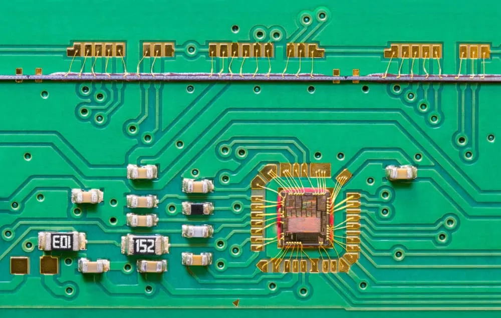
A printed wiring board, in its most precise technical definition, refers to the bare substrate with conductive pathways before any electronic components have been attached. The term emphasizes the interconnection function of the board, where copper traces serve as wiring that connects component mounting locations. This definition treats the PWB as the foundation or platform upon which a complete electronic assembly will be built, distinguishing it from the finished product that includes populated components.
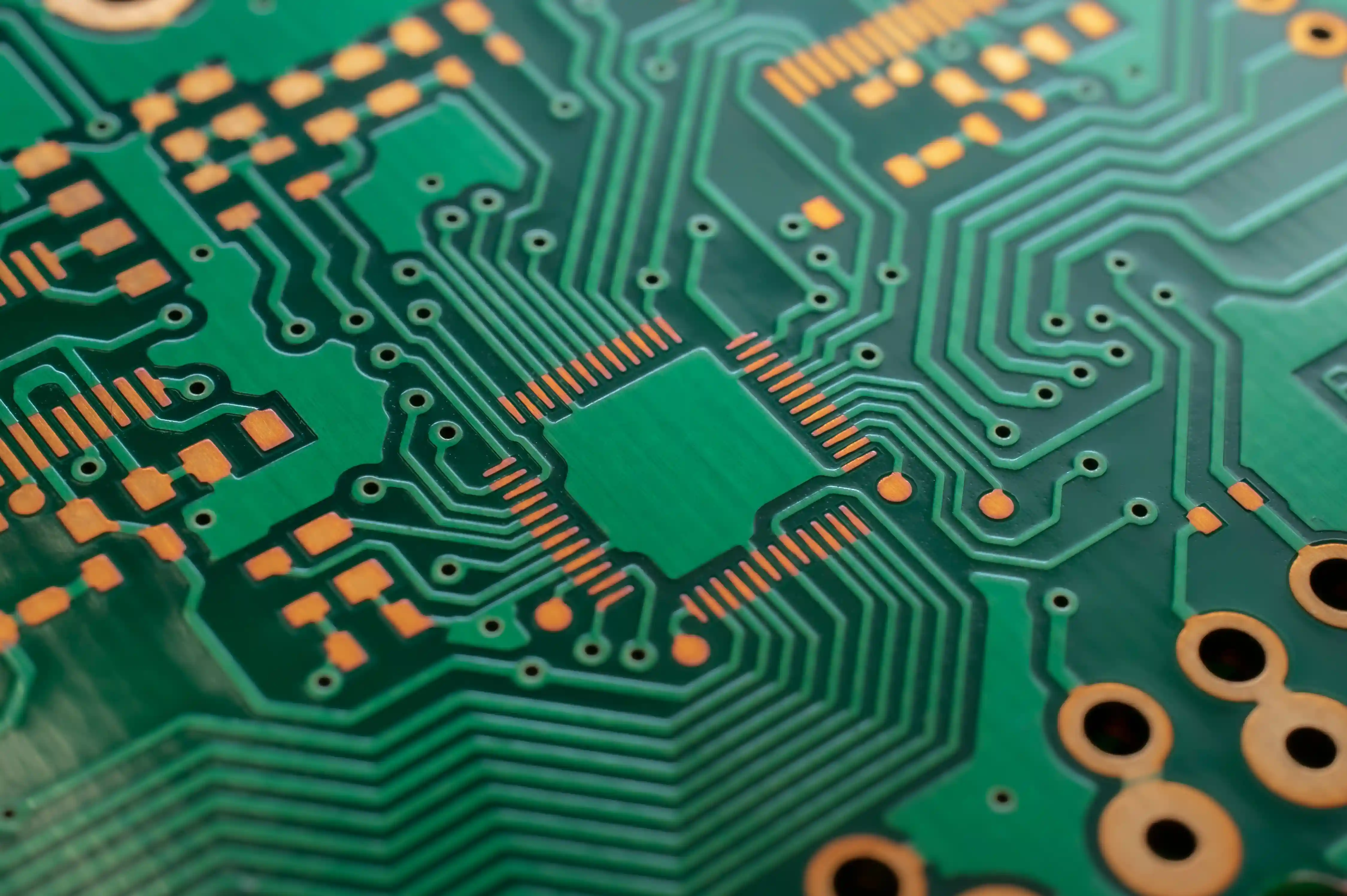
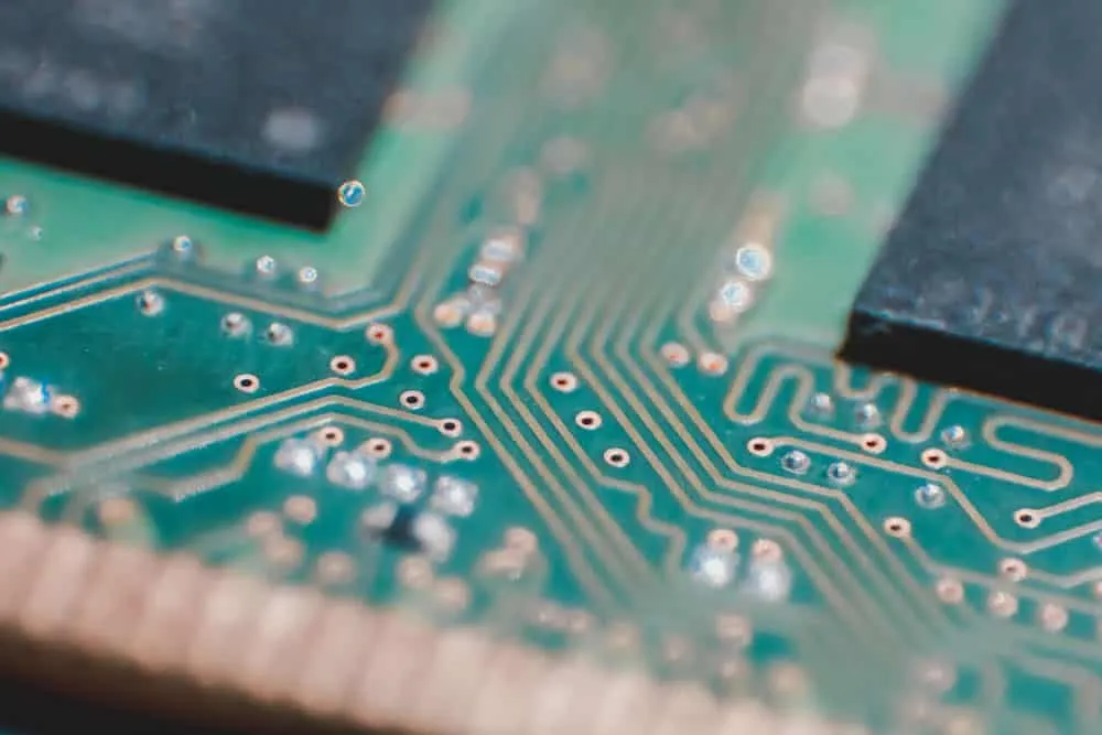
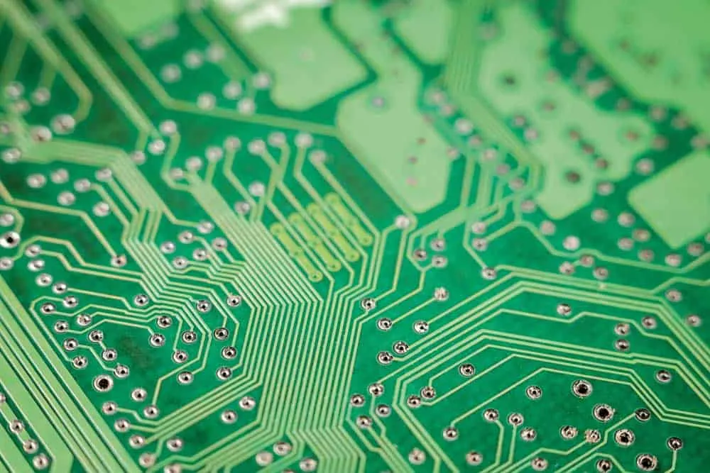
The construction of a printed wiring board begins with an insulating substrate material, most commonly FR-4 fiberglass-reinforced epoxy laminate. Copper foil bonds to one or both sides of this substrate, and selective removal of copper through etching processes creates the conductive trace patterns that form electrical interconnections. Additional processing steps add features like plated through-holes for layer connections, solder mask coating for protection, and surface finishes to enable component attachment.
Printed wiring boards emerged in the early 1950s as an alternative to point-to-point wiring that previously dominated electronic assembly. The ability to photographically reproduce wiring patterns and chemically etch them into copper foil revolutionized electronics manufacturing by enabling mass production of consistent, reliable interconnection substrates. This manufacturing approach established the foundation for the miniaturization and cost reduction that made modern consumer electronics possible.
PWB Versus PCB: Understanding the Distinction
The relationship between printed wiring board and printed circuit board terminology has evolved considerably over the decades since both terms entered common usage. Originally, the terms carried distinct meanings that reflected different stages in the electronic assembly process. A printed wiring board described the bare substrate with only the conductive traces, while a printed circuit board implied a more complete assembly including the components necessary to form functional circuits.
Modern usage has largely abandoned this distinction in most English-speaking markets. The Institute for Interconnecting and Packaging Electronic Circuits, known as IPC, formally adopted PCB as the standard term in 1999, effectively treating both terms as synonymous for most purposes. Today, PCB dominates usage in North America, Europe, and much of Asia, with printed wiring board appearing primarily in legacy documentation, formal specifications, or contexts where precise terminology matters.
Japan represents a notable exception to the global trend toward PCB terminology. Japanese manufacturers and documentation continue preferring PWB to avoid confusion with polychlorinated biphenyls, a group of toxic industrial chemicals commonly abbreviated as PCB in environmental and regulatory contexts. This linguistic consideration has kept PWB as the standard term throughout Japanese electronics industry communications, creating a persistent regional variation that international supply chains must accommodate.
Substrate Materials and Their Properties
The insulating substrate forms the mechanical foundation of any printed wiring board, providing structural support while maintaining electrical isolation between conductive layers. FR-4 glass-reinforced epoxy laminate dominates the industry due to its favorable combination of mechanical strength, electrical properties, thermal stability, and cost effectiveness. The material consists of woven fiberglass cloth impregnated with flame-retardant epoxy resin, creating a rigid platform suitable for most commercial electronic applications.
High-frequency applications demand substrate materials with superior electrical characteristics that FR-4 cannot provide. Polytetrafluoroethylene-based materials like Rogers laminates offer much lower dielectric constants and loss tangents, enabling signal integrity at frequencies where FR-4 would introduce unacceptable losses. Ceramic-filled PTFE composites provide even better performance for demanding RF and microwave circuits, though at significantly higher cost than standard materials.
Flexible printed wiring boards require entirely different substrate materials that can bend without cracking or delaminating. Polyimide films provide the flexibility needed for these applications while maintaining acceptable electrical properties and temperature resistance. Liquid crystal polymer substrates offer an alternative for applications requiring both flexibility and superior high-frequency performance, particularly in advanced antenna and sensor applications where traditional materials fall short.
Thermal management considerations increasingly influence substrate material selection as power densities rise in modern electronics. Metal-core printed wiring boards incorporate aluminum or copper base layers that conduct heat away from power components far more effectively than fiberglass laminates. Ceramic substrates provide even better thermal conductivity for the most demanding power applications, though their brittleness and processing requirements limit their use to specialized applications.
Layer Configurations and Construction
Printed wiring boards range from single-layer designs adequate for the simplest applications to complex multilayer structures containing dozens of individual copper layers. The choice of layer count depends on circuit complexity, component density, signal integrity requirements, and cost constraints. Understanding the capabilities and limitations of each configuration enables appropriate selection for specific application requirements.
Single-sided printed wiring boards carry copper traces on only one surface of the substrate, representing the simplest and most economical construction. Component leads insert through drilled holes and solder to pads on the copper side, while the opposite surface may carry silkscreen markings and solder mask but no conductive features. This configuration suits simple circuits where routing complexity permits all interconnections on a single layer.
Double-sided boards add copper to both substrate surfaces, roughly doubling available routing area and enabling more complex circuits. Plated through-holes connect traces between the two layers, allowing signals to transition from one side to the other as routing requirements dictate. Most consumer electronics products employ double-sided construction as it provides adequate complexity for typical applications while remaining cost-effective for volume production.
Multilayer printed wiring boards sandwich additional copper layers between the outer surfaces, with each internal layer separated by insulating prepreg material. Four-layer boards commonly dedicate internal layers to power and ground planes that provide low-impedance distribution and electromagnetic shielding for signal layers. Higher layer counts enable increasingly dense routing for complex digital circuits, with some advanced designs exceeding thirty layers for the most demanding applications.
Manufacturing Process Fundamentals
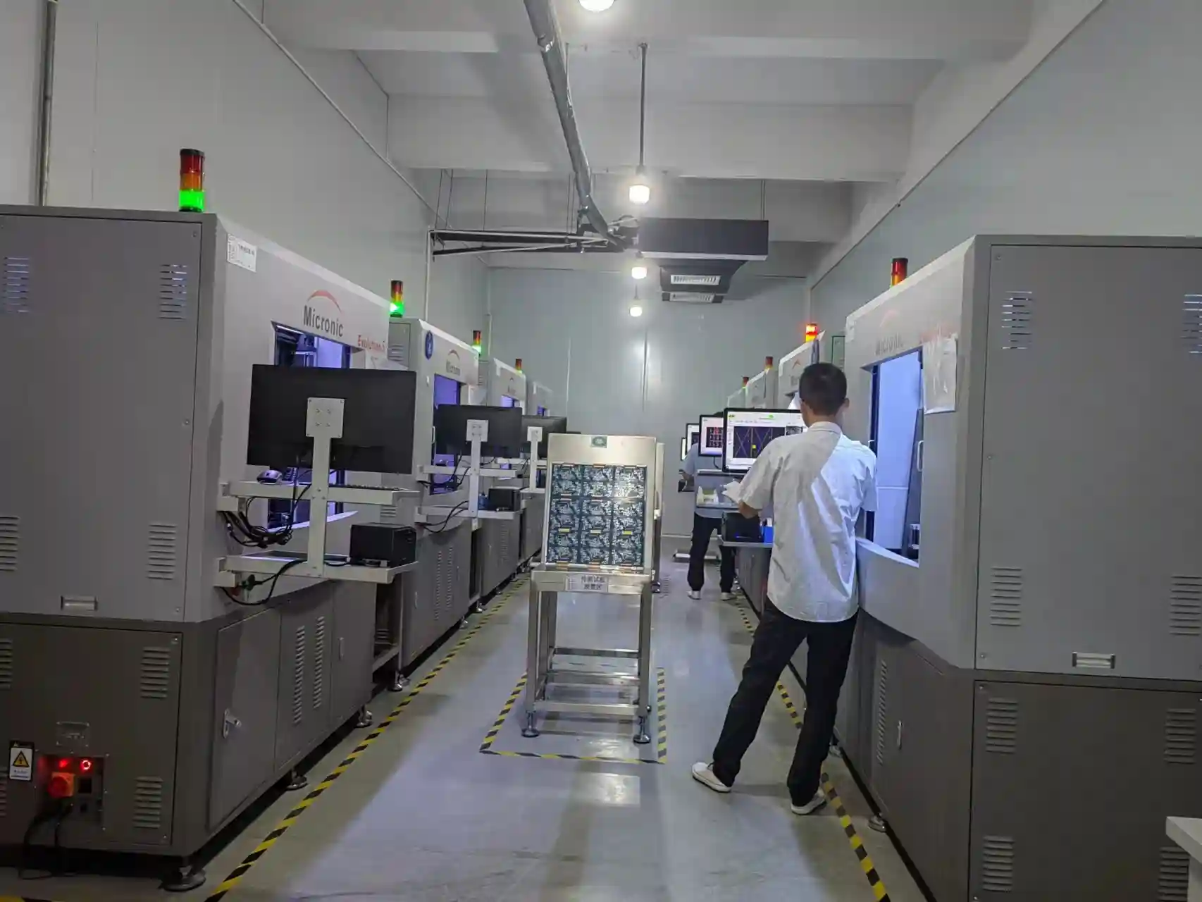
Printed wiring board fabrication involves a sequence of chemical, mechanical, and thermal processes that transform raw laminate material into finished interconnection substrates. The complexity of this process varies considerably depending on board specifications, with simple double-sided designs requiring far fewer steps than advanced multilayer constructions with controlled impedance requirements and fine-pitch features.
The manufacturing sequence typically begins with copper-clad laminate panels sized to accommodate multiple board images. A photosensitive dry film resist coats the copper surface, and exposure through photographic tooling transfers the circuit pattern to the resist. Development removes unexposed resist, leaving a protective pattern that shields the desired traces during subsequent etching. Chemical etching dissolves unprotected copper, and resist stripping reveals the finished trace pattern.
Drilling creates holes for through-hole components and interlayer connections called vias. Modern manufacturing uses computer-controlled drilling machines capable of producing thousands of holes per minute with positioning accuracy within a few micrometers. The drilled holes receive electroless copper plating followed by electrolytic copper buildup that creates the conductive barrel connecting copper layers on opposite sides of the board.
Multilayer construction requires lamination processes that bond individual layers into a unified structure. Inner layers undergo imaging and etching as separate panels before alignment and lamination with prepreg bonding material. Heat and pressure during lamination cure the prepreg epoxy, creating permanent bonds between layers. Subsequent drilling and plating create connections through the laminated structure, completing the electrical interconnections between all layers.
Factors Affecting Performance
Signal integrity becomes increasingly critical as operating frequencies rise in modern electronic systems. The dielectric constant of substrate materials directly affects signal propagation velocity, with lower dielectric constants enabling faster signal transmission. Trace geometry, including width, spacing, and relationship to reference planes, determines characteristic impedance that must match driver and receiver impedances to prevent reflections and signal degradation.
Power distribution networks within printed wiring boards must deliver stable supply voltages to all components despite varying current demands. Dedicated power and ground planes in multilayer constructions provide low-impedance paths that minimize voltage drops and supply noise. Strategic placement of decoupling capacitors supplements plane capacitance for high-frequency filtering that maintains supply stability during rapid switching transients.
Thermal management capabilities determine how effectively printed wiring boards can dissipate heat generated by power components. Standard FR-4 material conducts heat poorly, making thermal management challenging for high-power applications. Thermal vias, copper fills, and metal-core constructions improve heat spreading and conduction to external heatsinks. Proper thermal design prevents component overheating that would reduce reliability and shorten product life.
Mechanical considerations including board flatness, dimensional stability, and resistance to warping affect assembly yield and long-term reliability. Material selection, layer stackup symmetry, and processing parameters all influence mechanical behavior. Applications involving repeated flexing or thermal cycling impose additional requirements that standard rigid constructions may not satisfy, driving selection of specialized materials and constructions.
Quality and Reliability Considerations
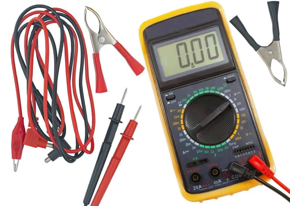
Printed wiring board quality encompasses both manufacturing defects detectable during production and latent weaknesses that may cause failures during product operation. Automated optical inspection identifies visible defects including trace opens, shorts, and dimensional deviations from specifications. Electrical testing verifies continuity and isolation for all networks, catching defects that may not be visually apparent.
Reliability testing subjects sample boards to accelerated stress conditions that reveal potential failure modes in compressed timeframes. Thermal cycling tests evaluate resistance to expansion and contraction stresses that occur during normal operation. Humidity and bias testing identifies susceptibility to electrochemical migration and insulation degradation. These qualification tests provide confidence that production boards will survive intended operating conditions throughout expected product life.
Industry standards from organizations including IPC define requirements for materials, processes, and finished board characteristics. IPC-6012 establishes qualification and performance specifications for rigid printed boards, defining classes with progressively stringent requirements. Class 1 applies to general electronic products where cosmetic imperfections are acceptable. Class 2 covers dedicated service electronics requiring extended life and reliable performance. Class 3 addresses high-reliability applications where failure is unacceptable.
Design Considerations for Manufacturability
Successful printed wiring board designs balance electrical performance requirements against manufacturing capabilities and cost implications. Design rules specifying minimum trace widths, spacing, hole sizes, and annular rings must fall within the capabilities of intended fabrication processes. Aggressive design rules that push manufacturing limits increase cost and may reduce yield, while conservative rules sacrifice density and may increase layer count.
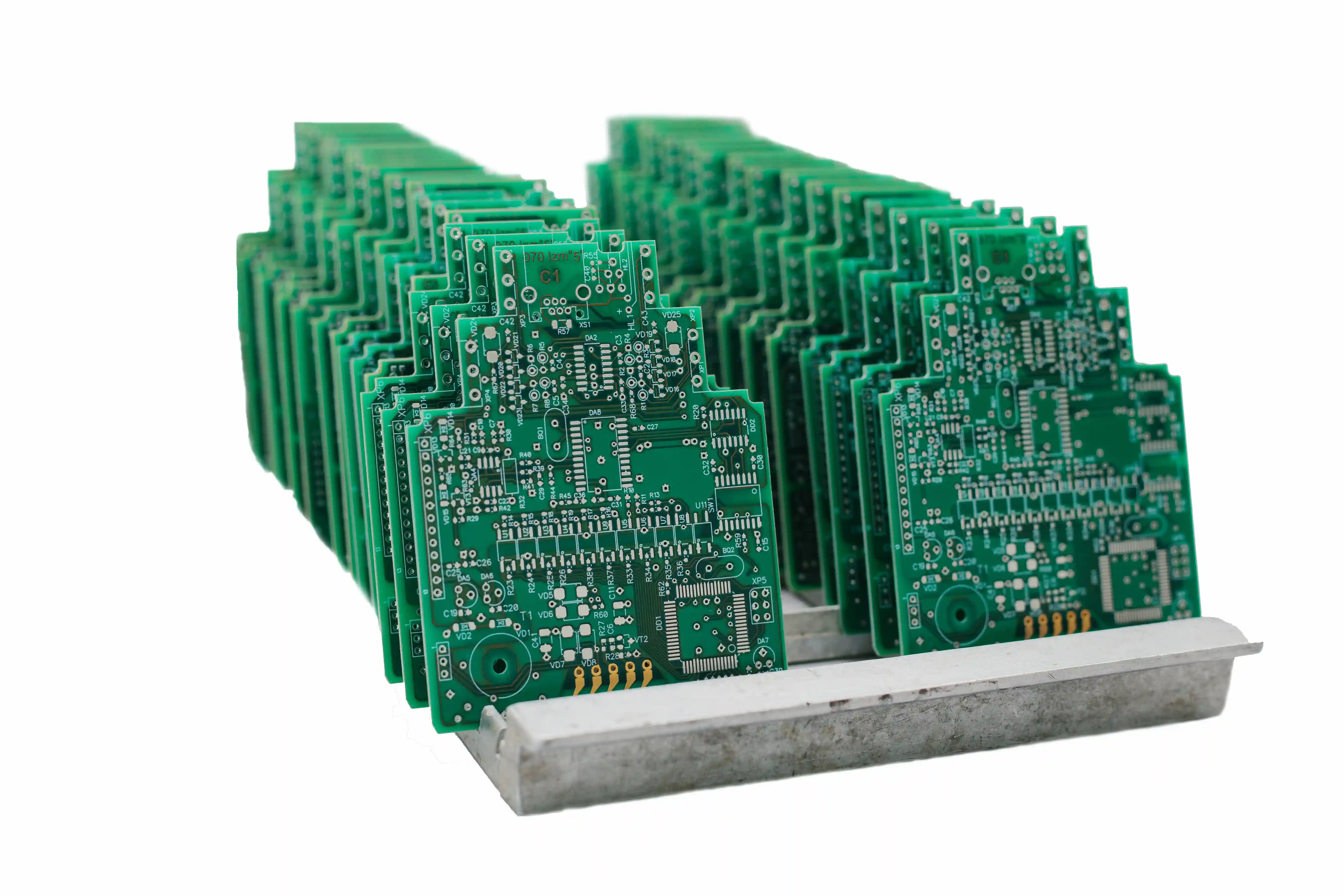
Panelization arranges multiple board images on manufacturing panels to optimize material utilization and processing efficiency. Small boards benefit particularly from panelization, as handling individual small pieces through processing equipment proves impractical. Breakaway tabs or V-score lines connect individual boards within panels, allowing separation after assembly. Panel design must consider handling requirements throughout the manufacturing and assembly process.
Documentation completeness significantly affects manufacturing success. Fabrication drawings specify all requirements not captured in electronic design files, including material specifications, surface finish requirements, controlled impedance values, and acceptance criteria. Incomplete or ambiguous documentation forces manufacturers to make assumptions that may not align with designer intentions, potentially resulting in boards that fail to meet actual requirements despite conforming to documented specifications.
Industry Applications and Requirements
Consumer electronics applications prioritize cost efficiency while maintaining adequate reliability for typical product lifetimes. Standard FR-4 material and Class 2 fabrication requirements satisfy most consumer product needs. Competitive pricing pressures drive designs toward minimum layer counts and relaxed design rules that maximize manufacturing yield and minimize material costs.
Automotive electronics demand significantly higher reliability given the extended operating life and harsh environmental conditions vehicles experience. Temperature extremes, vibration, humidity, and chemical exposure all stress automotive electronic assemblies. Specialized materials with extended temperature ratings, enhanced surface finishes, and Class 3 fabrication requirements address these challenges at increased cost compared to consumer-grade products.
Medical device applications impose unique requirements driven by regulatory considerations and the critical nature of healthcare equipment. Traceability requirements track material lots and processing parameters throughout manufacturing. Enhanced inspection and testing verify conformance to specifications with high confidence levels. Documentation requirements support regulatory submissions and enable investigations if field issues arise.
Aerospace and defense applications represent the most demanding segment, with requirements for extreme reliability under severe operating conditions. Specialized materials withstand temperature extremes and radiation exposure. Enhanced plating thicknesses and conformal coatings provide long-term protection. Extensive testing and qualification ensures boards meet stringent requirements before deployment in mission-critical systems.
Conclusion
Printed wiring boards form the essential interconnection foundation for virtually all modern electronic products. Whether called PWB or PCB, these substrates enable the dense, reliable, and cost-effective packaging that makes contemporary electronics possible. Understanding substrate materials, layer configurations, manufacturing processes, and quality considerations helps engineers and procurement professionals specify appropriate products for their applications.
The evolution from simple single-sided boards to complex multilayer structures with dozens of layers reflects the relentless advancement of electronic technology. As component densities continue increasing and operating frequencies rise, printed wiring board technology must advance correspondingly. Material developments, manufacturing process improvements, and design tool enhancements continue pushing the boundaries of what these essential building blocks can achieve.
For professional printed wiring board fabrication and assembly services meeting the highest quality standards, contact WellPCB for a customized quote addressing your specific requirements.
Frequently Asked Questions
What is the main difference between PWB and PCB?
In precise technical usage, PWB refers to the bare board substrate with conductive traces but no components, while PCB can refer to either bare boards or populated assemblies. However, modern industry practice largely treats these terms as interchangeable, with PCB being the dominant term in most English-speaking markets. Japan continues preferring PWB to avoid confusion with polychlorinated biphenyls.
Why does Japan use PWB instead of PCB?
Japanese industry adopted PWB to prevent confusion with polychlorinated biphenyls, toxic chemicals also abbreviated as PCB that remain subject to significant environmental regulation. Using PWB for printed wiring boards and PCB only for the chemical compound maintains clarity in documentation, regulatory submissions, and international communications involving Japanese companies.
What substrate materials are used for printed wiring boards?
FR-4 fiberglass-reinforced epoxy laminate dominates standard applications due to its balance of performance, reliability, and cost. High-frequency applications require low-loss materials like PTFE-based Rogers laminates. Flexible circuits use polyimide or liquid crystal polymer films. High-power applications may employ metal-core or ceramic substrates for improved thermal conductivity.
How many layers can a printed wiring board have?
Commercial printed wiring boards commonly range from one to twelve layers, with four and six-layer constructions being particularly common for moderate complexity designs. Advanced applications in computing, telecommunications, and aerospace regularly employ boards with twenty or more layers. Some extreme designs exceed forty layers, though such constructions require specialized manufacturing capabilities.
What factors affect printed wiring board cost?
Layer count has the greatest impact on cost, as each additional layer requires separate imaging, etching, and lamination processing. Board size, quantity, lead time, material selection, surface finish, and design rule aggressiveness all influence pricing. Controlled impedance requirements, via specifications, and quality class requirements add further cost factors that must be considered during design.
Related Articles
Continue exploring similar topics
AOI Testing Guide: PCB Automated Optical Inspection Explained
Complete guide to Automated Optical Inspection (AOI) for PCB manufacturing. Learn how AOI works, defect detection capabilities, 2D vs 3D systems, and implementation best practices.
Bed of Nails Test Fixture Guide: PCB In-Circuit Testing Explained
Complete guide to bed of nails test fixtures for PCB testing. Learn about fixture types, pogo pins, ICT procedures, and quality control applications.
Double-Sided PCB: Complete Design and Manufacturing Guide
Master double-sided PCB design with our comprehensive guide covering manufacturing processes, layout strategies, via specifications, and cost optimization tips.
Ready to bring your PCB design to life?
Get an instant quote for your custom PCB fabrication and assembly needs.
Get Instant Quote