
PCB Potting Guide: Compounds, Processes & Professional Services
Complete guide to PCB potting services. Learn about potting compounds, application processes, design considerations, and testing for encapsulated assemblies.
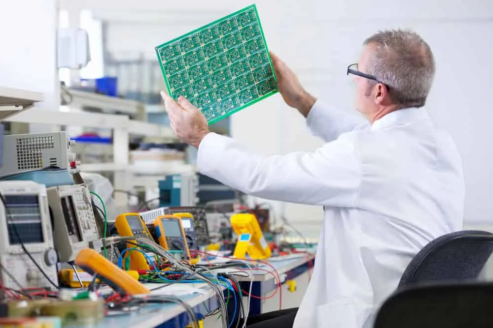
PCB potting encapsulates electronic assemblies in protective compounds, shielding circuits from moisture, vibration, contaminants, and impact damage. This process transforms bare circuit boards into rugged sealed modules capable of withstanding harsh operating environments. Professional potting services apply specialized expertise and equipment to deliver fully tested, protected assemblies. This comprehensive guide covers potting materials, processes, design considerations, and quality validation.
What is PCB Potting?
Potting is the process of completely encapsulating a PCB assembly within a liquid resin or polymer compound that cures to a solid protective block. This creates a dense, non-conductive barrier fortifying electronics against environmental and mechanical stresses.
The potting process involves:
1. Designing fixtures to hold PCBs and mask protected areas 2. Selecting potting compound chemistry suited to requirements 3. Mixing, degassing, and preparing materials 4. Loading boards into fixtures 5. Dispensing or injecting liquid potting material 6. Curing through heat, UV exposure, or chemical reaction 7. Inspecting for complete fill and proper curing 8. Testing potted assemblies for function and durability
Potting transforms bare circuits into sealed modules that withstand conditions destroying unprotected electronics.
Benefits of PCB Potting
Environmental Protection
Potting seals electronics from water, humidity, dust, chemicals, and corrosive contaminants. The solid barrier prevents moisture ingress that causes corrosion and short circuits over time.
Mechanical Protection
Hardened potting material buffers against vibration, shock, and impact damage during operation. Components remain secure despite mechanical stresses that would fatigue solder joints on unprotected boards.
Electrical Insulation
Potting electrically insulates components and prevents short circuits. High-voltage boards particularly benefit from the dielectric properties of potting compounds isolating conductors at different potentials.
Improved Thermal Performance
Quality potting compounds facilitate heat transfer away from components, aiding cooling when designed with appropriate thermal paths. Continuous contact between components and enclosure surfaces improves heat dissipation compared to air gaps.
EMI/RFI Shielding
Some potting materials incorporate conductive fillers providing electromagnetic and radio frequency interference shielding. This protects sensitive circuits from external interference while containing emissions.
Structural Reinforcement
Potting reinforces PCBs and components preventing flexing damage. Bonding strengthens solder joint fatigue resistance, extending product life under mechanical stress.
Security and Aesthetics
Opaque potting compounds conceal underlying circuit complexity, protecting intellectual property while providing uniform appearance. Reverse engineering becomes significantly more difficult.
Industries Using PCB Potting
Automotive
Under-hood controllers and power modules endure vibration, temperature cycling, and moisture exposure. Potting protects electronics surviving harsh engine compartment environments.
Aerospace
Avionics control systems face mechanical stresses, wide temperature swings, and altitude pressure changes. Potted assemblies maintain reliability through demanding flight conditions.
Marine Electronics
Humid, salty marine environments accelerate corrosion. Potting provides essential protection for navigation, communication, and control electronics on vessels.
Military and Defense
Mission-critical systems require hardening against shock, water, EMI, and environmental contaminants. Potted modules meet stringent military reliability requirements.
Medical Devices
Implantable and patient-contact devices require protection from body environment while preventing electrical hazards. Biocompatible potting compounds enable safe, reliable medical electronics.
Industrial Equipment
Process control electronics encounter dust, chemicals, and mechanical abuse during factory operation. Potting enables reliable automation despite harsh manufacturing environments.
Consumer Electronics
Products like outdoor cameras, power tools, and waterproof devices require improved robustness and liquid sealing. Potting delivers consumer-grade environmental protection.
Potting Compound Materials
Epoxy Resins
Most versatile and widely used potting material offering excellent adhesion, environmental resistance, and durability at reasonable cost. General-purpose epoxies operate continuously up to 150°C, while specialized high-temperature formulations withstand 180-200°C or higher.
- Advantages:
- Excellent adhesion to various substrates
- Strong chemical resistance
- Good electrical insulation properties
- Cost-effective for most applications
- Limitations:
- Rigid cure may stress sensitive components
- Longer curing times than some alternatives
- Difficult to remove for repairs
Polyurethane
Very tough protection with high impact and abrasion resistance. Flexible formulations address shortcomings of rigid epoxy for protecting circuits from physical stress. Greater adaptability suits various substrates including metals, ceramics, and polyimides.
- Advantages:
- Superior impact and abrasion resistance
- Flexible formulations absorb vibration
- Better stress absorption than epoxy
- Good moisture resistance
- Limitations:
- Typically opaque appearance
- Lower temperature resistance than silicone
- May require primers for some substrates
Silicone
Excellent high-temperature stability up to 200°C while maintaining flexibility. Good electrical insulation properties suit applications with thermal cycling concerns.
- Advantages:
- Wide temperature range tolerance
- Maintains flexibility after curing
- Excellent thermal stability
- Good stress relief properties
- Limitations:
- Higher moisture permeability than epoxy
- More expensive than alternatives
- Lower mechanical strength
Parylene
Very conformal pinhole-free thin coating applied via vapor deposition. Excels at moisture and chemical resistance with extremely uniform coverage.
- Advantages:
- Ultra-thin uniform coating
- Excellent chemical resistance
- Superior moisture barrier
- Biocompatible formulations available
- Limitations:
- Specialized deposition equipment required
- Higher cost per unit area
- Limited thickness capability
Rigid Black Compounds (RBC)
Opaque compounds containing epoxy and silicone providing very rigid, strong protection. High EMI/RFI shielding capability with excellent structural integrity.
Potting Process Techniques
Dispensing
Manually or automatically applies potting material in beads, fillets, or controlled deposits using pneumatic or electric dispensers. Allows selective application to specific zones requiring protection while leaving other areas accessible.
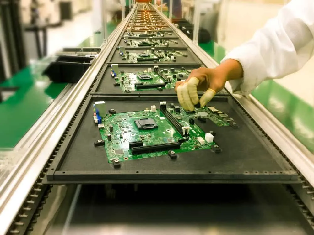
Encapsulation
Complete PCB placement in mold cavity with liquid potting material injected to surround the entire board. Creates uniform complete coverage for maximum protection.
Glob Top
Dispensing potting material over chip packages and wire bonds to protect IC components and delicate connections. Common for protecting bare die assemblies and sensitive semiconductors.
Underfill
Potting material dispensed under large BGAs and area array components for mechanical strengthening before curing. Improves thermal cycling reliability and drop resistance.
Casting
Pouring two-part potting mixture around assemblies in molds, similar to encapsulation but often with simpler tooling for lower volumes.
Vapor Deposition
Parylene coatings applied using vaporization chambers depositing polymer uniformly across all exposed surfaces. Provides conformal coverage of complex geometries.
Design Considerations for Potted PCBs
Avoiding Air Entrapment
Include vent holes allowing air evacuation during filling. Design generous fillets and radii in keepout zones preventing bubble trapping.
Containment Design
Design potting dams and containment walls limiting fill area. Specify fill ports and air evacuation locations enabling complete coverage.
Component Considerations
- - Mechanically secure components before potting
- Position tall components avoiding tilting when submerged
- Specify toughened solder mask resisting cracking
- Mark heat sinks and connectors remaining exposed
Thermal Management
Specify thermal vias under hot components enabling heat transfer through potting material. Ensure potting contacts heat sinks and chassis surfaces for effective thermal paths.
Thickness Guidelines
- - Minimum 3mm potting thickness over components provides sufficient mechanical strength
- 2mm thickness typical for PCB coverage
- Adjust based on specific environmental requirements
Common Potting Issues
Voids
Air trapped during filling or insufficient material results in unprotected voids. Slow filling, proper venting, and degassing prevent bubble formation.
Cracks
Cracking occurs when using inflexible compounds with fragile components or PCBs. Thermal expansion differences between materials also cause cracks. Material selection matching component and substrate properties prevents cracking.
Component Shifting
Tall, heavy components tilt or fall over during filling before compound hardens. Mechanical securing before potting prevents movement.
Wicking
Potting material adheres up component bodies away from PCB surface, leaving areas unprotected. Material selection and application technique control wicking.
Outgassing
Some compounds release gas bubbles during curing, creating pockets. Proper mixing, slow filling, adequate venting, and gradual temperature ramping allow gases to escape.
Amine Bloom
Two-component epoxy absorbs moisture from air, creating mottled surface appearance. Fresh compounds stored in low-humidity, temperature-controlled environments prevent this issue.
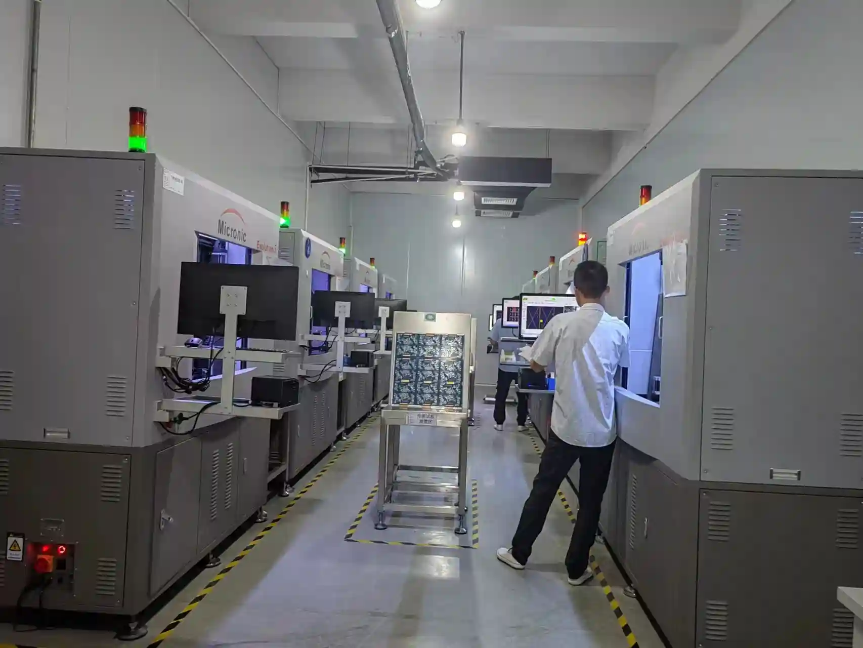
Testing Potted Assemblies
Visual Inspection
Checks for complete filling, air gaps, wicking issues, and cosmetic defects. First-line quality verification.
Dimensional Inspection
Verifies height, length, width, and component placement tolerances maintain after potting.
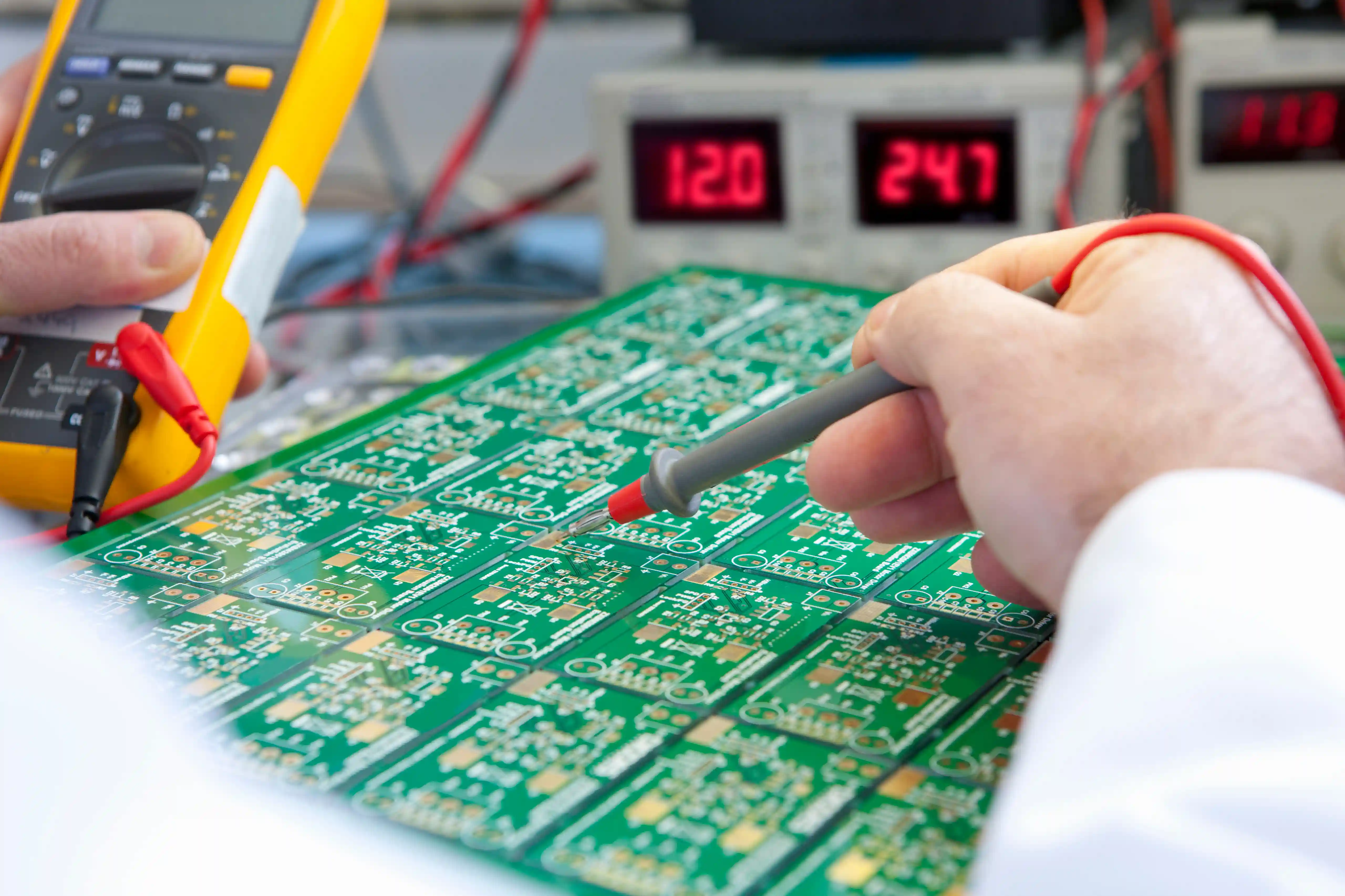
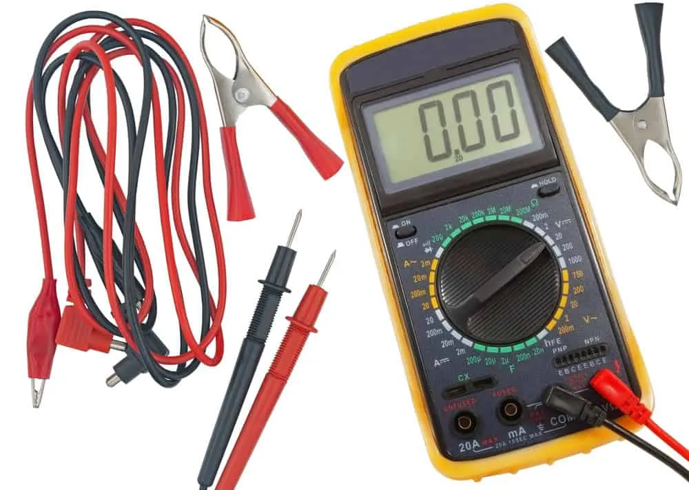
Electrical Testing
ICT fixtures or flying probes perform in-circuit testing validating all functions operate correctly. Burn-in testing may verify long-term reliability.
Mechanical Testing
Vibration, shock, and torque testing determines if cracks or delamination indicate potting defects.
Hermeticity Testing
Per IPC standards, confirms complete moisture seal preventing environmental ingress.
Thermal Cycling
Temperature ramps with electrical testing during cycling checks for intermittent failures from material stress.
Dielectric Testing
Measurement of dielectric strength, insulation resistance, and capacitance verifies electrical integrity.
Benefits of Professional Potting Services
Outsourcing to experienced potting service providers offers significant advantages:
- - Specialized potting fixtures, molds, and dispensing equipment
- Expertise selecting compatible materials and processes
- Precision dispensing and injection molding capabilities
- Established cleaning, curing, and inspection procedures
- Mass production and small batch prototyping capabilities
- Testing expertise validating potted assembly function
- Skills performing selective techniques like glob tops
- Design assistance optimizing boards for potting
- Troubleshooting issues like voids, cracks, and filler errors
Summary
PCB potting encapsulates assemblies in protective compounds providing environmental, mechanical, and electrical protection for challenging operating conditions. Various potting compounds—epoxy, polyurethane, silicone, parylene—offer specific benefits matching application requirements. Professional potting services apply specialized expertise and equipment delivering fully tested, protected assemblies ready for deployment in harsh environments.
For professional PCB potting services and expert guidance on protective encapsulation, contact WellPCB for competitive quotes and quality solutions.
Frequently Asked Questions
What potting materials provide the best moisture protection?
Epoxies offer very low moisture permeability and excellent adhesion preventing water ingress. Flexible polyurethanes and rigid black compounds also provide strong water resistance. Parylene delivers exceptional moisture barrier performance for thin-coating applications.
How is outgassing prevented when potting PCBs?
Outgassing minimizes through proper mixing, slow filling, adequate venting, and gradual cure temperature ramping allowing gases to escape from resin. Choosing potting compounds with low volatility also helps prevent bubble formation.
Does potting increase or decrease thermal resistance?
Potting generally improves heat transfer when providing continuous thermal conduction paths to heat sinks and chassis. However, air pockets trapped during filling increase thermal resistance. Proper process technique ensures solid thermal contact.
How thick should potting be over components?
Minimum 3mm potting thickness over components provides sufficient mechanical strength. For PCB surfaces, 2mm thickness is typical. Thickness may increase based on specific environmental severity, vibration levels, or impact protection requirements.
Can potted assemblies be repaired?
Most potted assemblies cannot be practically repaired as removing cured compound damages circuits. Silicone compounds allow limited surgical removal, but design should assume potting is permanent. Thorough testing before potting prevents field repair requirements.
Related Articles
Continue exploring similar topics
AOI Testing Guide: PCB Automated Optical Inspection Explained
Complete guide to Automated Optical Inspection (AOI) for PCB manufacturing. Learn how AOI works, defect detection capabilities, 2D vs 3D systems, and implementation best practices.
Bed of Nails Test Fixture Guide: PCB In-Circuit Testing Explained
Complete guide to bed of nails test fixtures for PCB testing. Learn about fixture types, pogo pins, ICT procedures, and quality control applications.
Double-Sided PCB: Complete Design and Manufacturing Guide
Master double-sided PCB design with our comprehensive guide covering manufacturing processes, layout strategies, via specifications, and cost optimization tips.
Ready to bring your PCB design to life?
Get an instant quote for your custom PCB fabrication and assembly needs.
Get Instant Quote