PCB Encapsulation Guide: Materials, Techniques & Benefits
Complete guide to PCB encapsulation and potting. Learn materials, application methods, benefits, and when to choose encapsulation over conformal coating.
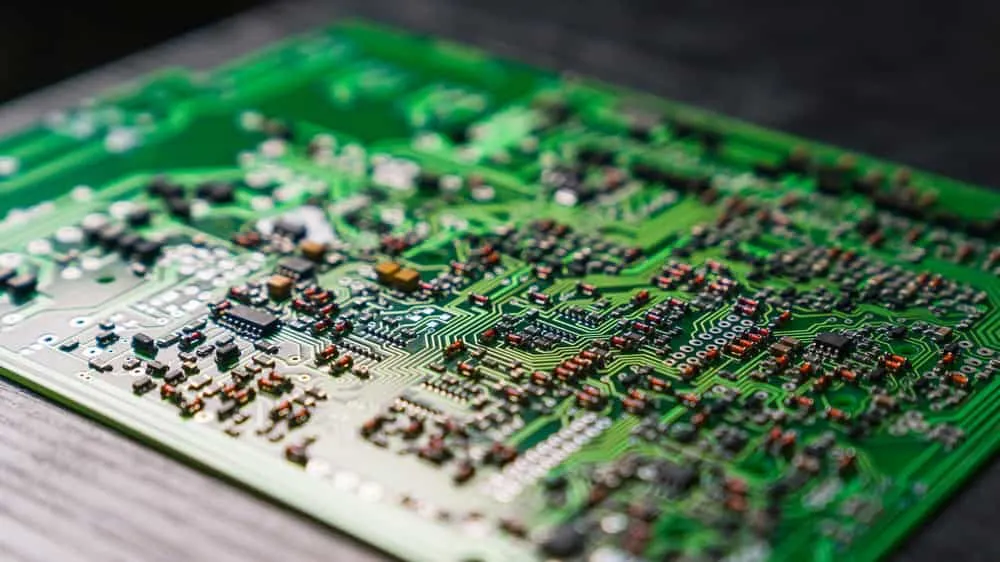
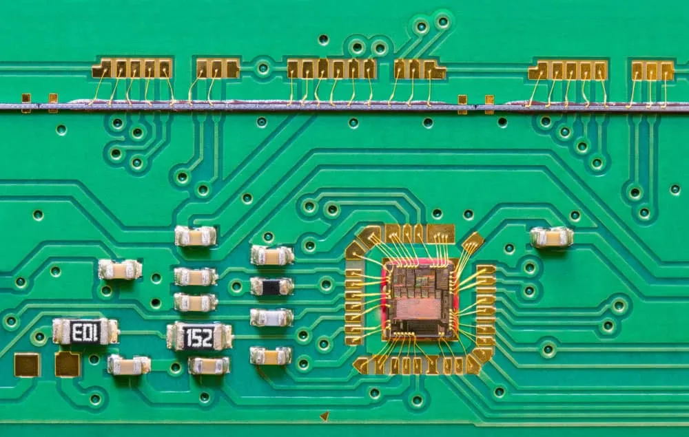
PCB encapsulation provides robust protection for electronic assemblies operating in demanding environments. This process involves surrounding printed circuit boards with protective compounds that shield against moisture, chemicals, vibration, mechanical shock, and environmental contaminants. Understanding encapsulation materials, techniques, and applications helps designers select appropriate protection methods for their specific requirements.
What is PCB Encapsulation?
PCB encapsulation surrounds electronic assemblies with protective compounds providing comprehensive defense against environmental hazards. Unlike conformal coating that applies thin protective films, encapsulation creates thick protective shells typically ranging from 1-10 millimeters. The process involves placing PCB assemblies inside enclosures or molds, then filling completely with liquid potting compounds that cure into solid protective barriers.
The terms encapsulation and potting are often used interchangeably, though technically they describe slightly different processes. Potting typically involves creating a case or shell, then pouring resin over the assembly so the container becomes part of the final product. Encapsulation may involve complete immersion in compound without permanent housing. Both processes achieve similar protective outcomes through thick polymer barriers surrounding sensitive electronics.
Encapsulation compounds typically consist of two-part systems mixing resin and hardener. This chemical reaction creates cross-linked polymers providing mechanical strength, chemical resistance, and environmental sealing. Many formulations cure at room temperature without requiring heat or specialized equipment, simplifying production processes for manufacturers.
PCB Encapsulation vs. Conformal Coating
Choosing between encapsulation and conformal coating depends on application requirements, environmental conditions, and operational constraints. Neither method is universally superior—each suits specific circumstances.
| Factor | Conformal Coating | Encapsulation | |--------|------------------|---------------| | Thickness | 25-250 micrometers | 1-10 millimeters | | Weight Impact | Minimal | Significant increase | | Mechanical Protection | Moderate | Excellent | | Shock/Vibration Resistance | Basic | Superior | | Reworkability | Good—removable | Difficult—permanent | | Cost | Lower | Higher | | Application Speed | Faster | Slower | | Visibility | Components visible | Components hidden |
When to Choose Conformal Coating
Conformal coating suits applications requiring flexibility, reworkability, and minimal weight impact. Consumer electronics, mobile devices, and products requiring field repairs benefit from thin protective films allowing component access. Coating provides adequate protection against humidity, dust, and light environmental exposure without the weight and permanence of encapsulation.
When to Choose Encapsulation
Encapsulation excels in harsh environments demanding maximum protection. Industrial equipment, outdoor installations, automotive electronics, mining equipment, and power plant controls face extreme conditions where thick protective barriers prove essential. High-voltage applications benefit from encapsulation's superior dielectric properties preventing electrical arcs. Products requiring tamper resistance or intellectual property protection leverage the visual barrier preventing component identification.
Encapsulation Materials
Epoxy Encapsulants
Epoxy compounds provide excellent chemical resistance, high adhesion strength, and superior mechanical protection. These materials cure into hard, rigid barriers protecting against physical impact and environmental exposure. Epoxy works well for high-temperature applications where thermal stability proves critical.
- Advantages:
- Excellent chemical resistance
- Superior mechanical strength
- Good thermal conductivity options
- Strong adhesion to various substrates
- Limitations:
- Rigid cure may stress sensitive components
- Longer curing times than alternatives
- Difficult to remove for repairs
Silicone Encapsulants
Silicone compounds offer flexibility across extreme temperature ranges, making them ideal for applications experiencing thermal cycling. These materials maintain elasticity from -55°C to +200°C, accommodating thermal expansion without stressing components. Silicone provides excellent moisture resistance and electrical insulation.
- Advantages:
- Wide temperature range tolerance
- Excellent flexibility and stress relief
- Superior moisture resistance
- Good electrical insulation
- Limitations:
- Higher cost than alternatives
- Lower mechanical strength
- Lower chemical resistance to solvents
Polyurethane Encapsulants
Polyurethane provides balanced properties between rigid epoxy and flexible silicone. These compounds offer good chemical resistance, reasonable flexibility, and effective moisture protection at moderate cost. Polyurethane works well for applications requiring protection without extreme temperature exposure.
- Advantages:
- Balanced flexibility and strength
- Good chemical resistance
- Reasonable cost
- Faster curing than epoxy
- Limitations:
- Temperature limitations compared to silicone
- May yellow with UV exposure
- Lower thermal conductivity
Material Selection Criteria
Selecting appropriate encapsulation materials requires evaluating operating conditions:
- - Temperature range: Silicone for extreme thermal cycling, epoxy for high sustained temperatures
- Chemical exposure: Epoxy for solvent resistance, polyurethane for general chemical protection
- Mechanical stress: Epoxy for rigid protection, silicone for shock absorption
- Cost constraints: Polyurethane offers balanced performance at moderate cost
- Thermal management: Thermally conductive formulations available in all material types
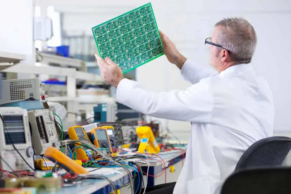
PCB Encapsulation Process
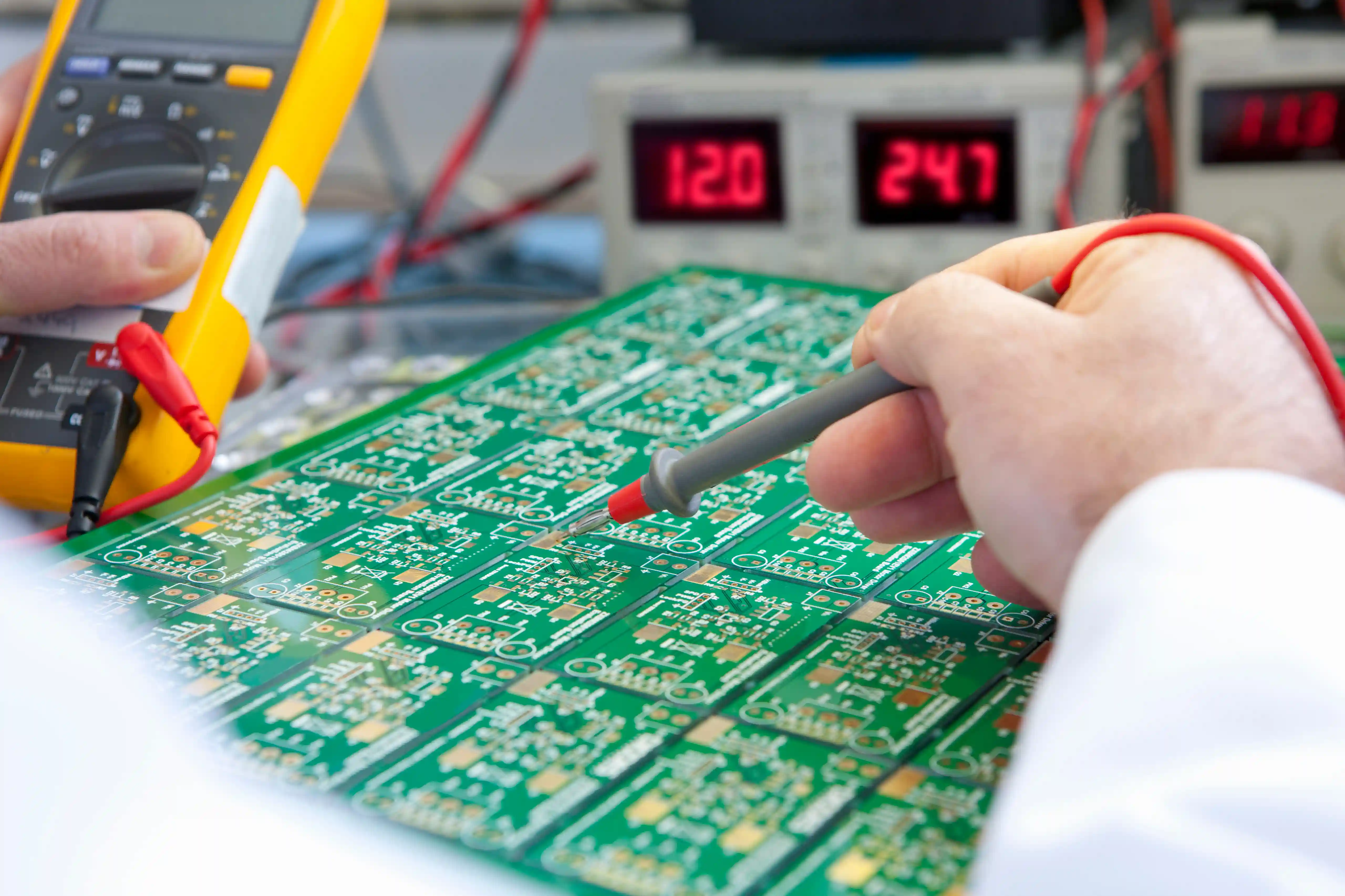
Preparation Steps
Successful encapsulation requires thorough preparation ensuring compound adhesion and complete coverage:
1. Surface Cleaning: Remove flux residues, contaminants, and oils that could prevent adhesion or create voids 2. Moisture Removal: Bake assemblies to eliminate absorbed moisture that could cause bubbles during cure 3. Masking: Protect connectors, test points, and areas requiring post-encapsulation access 4. Mold Preparation: Prepare enclosures or molds with release agents if removal is intended
Application Methods
Manual Potting: Operators pour mixed compound into enclosures containing PCB assemblies. Suitable for low-volume production and custom configurations. Quality depends on operator skill and attention to complete coverage.
Automated Dispensing: Programmable systems meter and dispense precise compound quantities. Provides consistency for medium to high-volume production while reducing material waste and labor costs.
Vacuum Potting: Drawing vacuum during encapsulation removes trapped air and ensures complete penetration around components. Essential for dense assemblies where air pockets could compromise protection or create dielectric weaknesses.
Curing Process
Most encapsulation compounds cure through chemical reaction between resin and hardener components. Cure profiles vary by material:
- - Room temperature cure: Many formulations solidify within 24-72 hours at ambient temperature
- Heat accelerated cure: Elevated temperature reduces cure time to hours or minutes
- UV cure: Specialized formulations cure rapidly under ultraviolet light exposure
Proper cure ensures full material properties develop. Incomplete curing leaves compounds soft or tacky with reduced protective capabilities.
Benefits of PCB Encapsulation
Environmental Protection
Encapsulation creates sealed barriers preventing moisture, chemicals, dust, and contaminants from reaching sensitive electronics. This protection enables reliable operation in outdoor environments, industrial facilities, and applications exposed to harsh conditions that would quickly damage unprotected assemblies.
Mechanical Protection
Thick encapsulation layers absorb mechanical shock and dampen vibration that could fracture solder joints or damage fragile components. Wire bonds, surface mount connections, and through-hole joints all benefit from reduced mechanical stress. Products survive shipping, handling, and operational vibration that would damage exposed assemblies.
Electrical Improvements
Encapsulation compounds provide excellent dielectric properties preventing electrical arcs in high-voltage applications. Improved insulation between conductors enables reliable operation at elevated voltages. Reduced current leakage improves efficiency while preventing safety hazards.
EMI/RFI Shielding
Specialized encapsulation compounds incorporating conductive fillers provide electromagnetic interference shielding. This reduces both emissions from circuits and susceptibility to external interference, enabling compliance with electromagnetic compatibility requirements.
Thermal Management
Thermally conductive encapsulation compounds transfer heat from components to enclosure surfaces for dissipation. This capability proves valuable for power electronics and LED assemblies where thermal management directly affects performance and longevity.
Tamper Resistance
Opaque encapsulation compounds conceal circuit designs from visual inspection, protecting intellectual property and preventing reverse engineering. Physical protection also prevents tampering with security-critical electronics where unauthorized modification could compromise system integrity.
Tin Whisker Prevention
Encapsulation creates environmental barriers preventing tin whisker growth—metallic filaments that can cause short circuits in tin-finished assemblies. This protection proves particularly valuable for high-reliability applications in aerospace and medical electronics.
Applications of PCB Encapsulation
Industrial Electronics
Manufacturing environments expose electronics to vibration, dust, moisture, and chemical contamination. Encapsulated controllers, sensors, and power supplies operate reliably despite harsh factory conditions that would quickly compromise unprotected circuits.
Automotive Electronics
Vehicle electronics face extreme temperature ranges, vibration, moisture, and chemical exposure from fluids and road treatments. Encapsulation enables reliable operation throughout vehicle lifetimes despite demanding automotive environments.
Outdoor and Marine Equipment
Weather exposure, humidity, salt spray, and temperature cycling challenge outdoor electronics. Encapsulation provides long-term protection for communications equipment, lighting controls, solar inverters, and marine electronics operating in exposed locations.
Medical Devices
Medical electronics require protection enabling reliable operation during sterilization cycles and exposure to cleaning chemicals. Encapsulation also prevents contamination of sensitive environments by sealed electronics.
Power Electronics
High-voltage power supplies, inverters, and motor controllers benefit from encapsulation's excellent dielectric properties. Protection against electrical arcing and environmental contamination ensures safe, reliable operation at elevated voltages.
LED Lighting
LED assemblies generate significant heat while operating in exposed environments. Thermally conductive encapsulation transfers heat for dissipation while protecting electronics from moisture and contamination extending product life.
Cables and Connectors
Encapsulation protects cable terminations and connector assemblies from moisture ingress, mechanical stress, and environmental exposure. This extends service life for cables in demanding applications.
Industry Standards
Several standards govern encapsulation materials and applications:
- - IPC-CC-830C: Primary standard for conformal coatings on PCBs, covering material requirements, curing, shelf-life, viscosity, and resistance properties
- IPC-A-610J: Addresses coating coverage and thickness requirements for electronic assembly acceptability
- IPC-J-STD-001J: Details application, materials, thickness, and uniformity requirements for coatings and encapsulation
- UL 94: Flammability ratings for encapsulation materials
- RoHS/REACH: Environmental compliance for encapsulation compounds
Considerations and Limitations
Weight Increase
Encapsulation compounds add significant mass to assemblies. Weight-sensitive applications like aerospace and portable electronics must balance protection needs against weight constraints.
Rework Challenges
Once cured, encapsulation compounds cannot be easily removed for repairs or modifications. Design must account for component reliability since rework proves impractical. Some silicone compounds allow surgical removal, but most encapsulation effectively becomes permanent.
Heat Dissipation
Standard encapsulation compounds have lower thermal conductivity than air, potentially trapping heat within assemblies. Thermally conductive formulations address this concern for power-dissipating circuits.
Component Stress
Rigid encapsulation compounds may stress sensitive components during thermal cycling as differential expansion rates create mechanical forces. Flexible silicone compounds minimize this concern for applications experiencing temperature extremes.
Cost Considerations
Encapsulation materials, labor, and process time increase production costs compared to conformal coating. Evaluate whether protection requirements justify additional expense for specific applications.
Summary
PCB encapsulation provides comprehensive protection for electronics operating in demanding environments. Understanding material options, process requirements, and application considerations enables informed decisions balancing protection needs against cost, weight, and rework constraints. For harsh environments, high-voltage applications, or tamper-resistant requirements, encapsulation delivers protection levels exceeding conformal coating alternatives.
For professional PCB encapsulation services or assistance selecting appropriate protection methods, contact WellPCB for expert consultation and competitive quotes.
Frequently Asked Questions
What is the difference between potting and encapsulation?
The terms are often used interchangeably. Technically, potting involves creating a permanent case or shell that becomes part of the final product, while encapsulation may involve complete immersion in compound without permanent housing. Both achieve similar protective outcomes through thick polymer barriers.
Can encapsulated PCBs be repaired?
Rework proves extremely difficult or impossible for most encapsulated assemblies. Rigid epoxy compounds cannot be removed without damaging components. Some silicone formulations allow surgical removal, but design should assume encapsulation is permanent. Thorough testing before encapsulation prevents field repair requirements.
Which encapsulation material works best for high temperatures?
Silicone compounds offer the widest temperature range, maintaining properties from -55°C to +200°C. Specialized high-temperature epoxy formulations also tolerate elevated temperatures. Material selection should consider both maximum operating temperature and thermal cycling requirements.
How thick should PCB encapsulation be?
Typical encapsulation thickness ranges from 1-10 millimeters depending on protection requirements. Thicker layers provide greater mechanical protection and improved dielectric properties for high-voltage applications. Minimum thickness should cover all components with adequate margin for manufacturing variation.
Does encapsulation affect heat dissipation?
Standard encapsulation compounds have lower thermal conductivity than air, potentially trapping heat. Thermally conductive formulations with ceramic or metalite fillers address this concern, transferring heat from components to enclosure surfaces for dissipation. Material selection must consider thermal management requirements.
Related Articles
Continue exploring similar topics
AOI Testing Guide: PCB Automated Optical Inspection Explained
Complete guide to Automated Optical Inspection (AOI) for PCB manufacturing. Learn how AOI works, defect detection capabilities, 2D vs 3D systems, and implementation best practices.
Bed of Nails Test Fixture Guide: PCB In-Circuit Testing Explained
Complete guide to bed of nails test fixtures for PCB testing. Learn about fixture types, pogo pins, ICT procedures, and quality control applications.
Double-Sided PCB: Complete Design and Manufacturing Guide
Master double-sided PCB design with our comprehensive guide covering manufacturing processes, layout strategies, via specifications, and cost optimization tips.
Ready to bring your PCB design to life?
Get an instant quote for your custom PCB fabrication and assembly needs.
Get Instant Quote