GPU PCB Design Guide: Understanding Graphics Card Circuit Boards
Comprehensive guide to GPU PCB design covering layer structures, power delivery, thermal management, and how PCB quality affects graphics card performance.
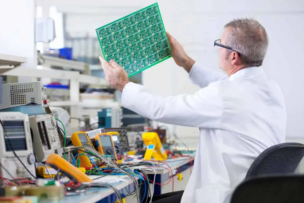
The printed circuit board forms the foundation of every modern graphics card, serving as the central nervous system connecting all components. As GPU technology has evolved from simple 2D accelerators to massively parallel processors capable of real-time ray tracing and AI acceleration, PCB complexity has grown exponentially. Understanding GPU PCB design helps enthusiasts, engineers, and buyers appreciate what distinguishes premium graphics cards from basic models.
What is a GPU PCB?
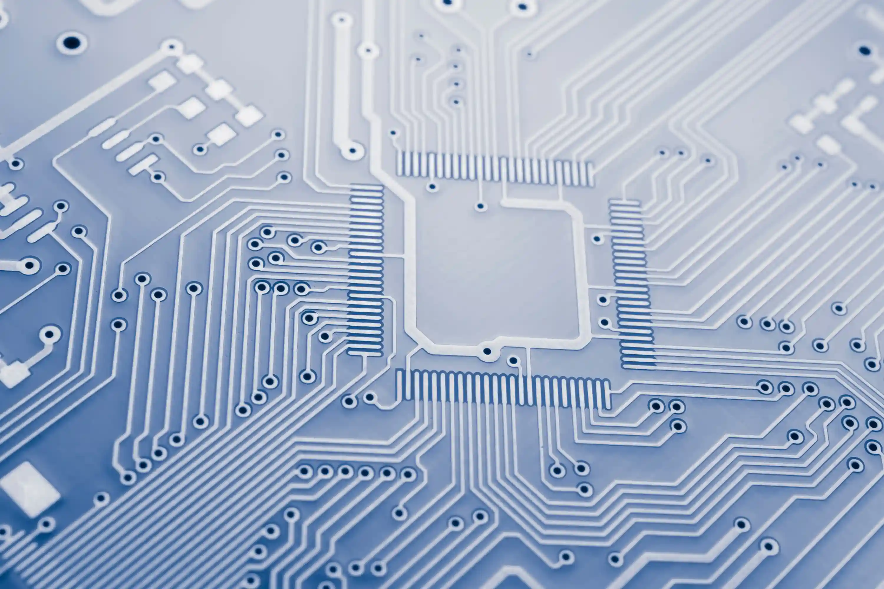
A GPU PCB (Printed Circuit Board) provides the physical platform connecting all graphics card components. Far more than a simple mounting surface, the PCB represents a carefully engineered system balancing electrical performance, thermal management, mechanical stability, and signal integrity. Modern high-end graphics cards like NVIDIA RTX 4090 or AMD RX 7900 XTX feature PCBs with 12-16 layers, sophisticated power delivery systems, and advanced cooling solutions handling 300-600W of power dissipation.
The PCB transforms raw silicon GPU chips into functional graphics cards by providing mounting surfaces for components, facilitating electrical communication through copper traces, delivering clean stable power to all circuits, and providing structural integrity for handling and installation. Without this carefully designed foundation, the most advanced GPU processors would remain inert silicon unable to achieve their spectacular performance capabilities.
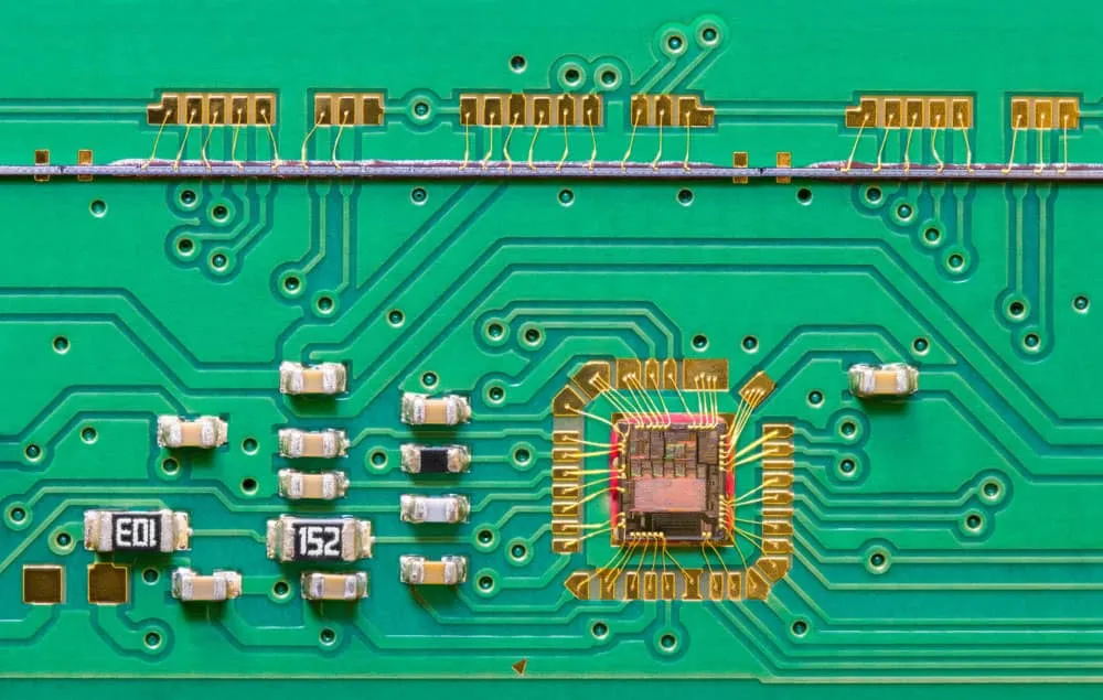
Key Components Mounted on GPU PCBs
GPU Chip (Graphics Processing Unit)
The GPU die represents the heart of any graphics card—a rectangular integrated circuit containing billions of transistors for processing graphics calculations and video rendering. Modern GPUs handle massively parallel workloads including gaming, professional visualization, machine learning, and cryptocurrency mining. The PCB must deliver substantial power to this component while dissipating considerable heat generated during operation.
Video Memory (VRAM)
VRAM chips surround the GPU die, providing high-bandwidth memory for storing textures, frame buffers, and working data. Modern cards use GDDR6, GDDR6X, or HBM memory requiring precise timing and power delivery. The PCB must maintain signal integrity across memory interfaces operating at speeds measured in gigabits per second while managing thermal considerations for densely packed memory chips.
Power Delivery System
Voltage Regulator Modules (VRMs) convert 12V power from the system into lower voltages required by GPU and memory circuits. Quality VRMs ensure smooth power delivery despite heavy, fluctuating loads that characterize gaming workloads. The power delivery section typically includes MOSFETs, chokes, and capacitors arranged in phases that work together distributing current demands.
Display Outputs and Connectors
PCIe edge connectors interface with motherboards for power and communication. Display outputs including HDMI, DisplayPort, and sometimes legacy DVI or VGA require dedicated circuitry and physical connectors. Power connectors (6-pin, 8-pin, or 12-pin configurations) supplement motherboard power for higher-wattage designs.
Support Circuitry
Additional components include BIOS chips storing firmware, display encoders converting digital signals for monitors, fan controllers managing cooling systems, and various filtering and protection components ensuring stable operation.
GPU PCB Design Considerations
Signal Integrity
Modern GPUs operate at clock speeds exceeding 2GHz with memory interfaces transferring data at 20+ Gbps. Maintaining signal integrity at these frequencies demands careful impedance tuning, controlled trace lengths, and strategic routing avoiding interference sources. Differential pair routing maintains timing precision for high-speed interfaces. Poor signal integrity causes data errors, crashes, and performance degradation that no amount of raw silicon performance can overcome.
Power Integrity
High-performance graphics cards consume 200-600W during intensive workloads, demanding robust power delivery with minimal ripple and noise. Power planes must handle high currents while maintaining voltage stability. Quality capacitors filter noise while providing instantaneous current during load transients. Insufficient power delivery causes voltage droops affecting stability, particularly during overclocking attempts.
Thermal Management
GPU dies generate substantial heat concentrated in small areas, often exceeding 200W from chips smaller than 500 square millimeters. The PCB must facilitate heat transfer to cooling solutions through thermal interface materials, thermal vias conducting heat between layers, and copper spreading heat across larger areas. Power delivery components also generate considerable heat requiring thermal consideration in board layout.
Component Placement
Optimal component placement balances multiple competing requirements including signal routing distances, thermal distribution, power delivery efficiency, and manufacturing feasibility. GPU and memory placement affects trace lengths impacting signal timing. VRM location affects both power delivery efficiency and thermal management. Connector placement affects card dimensions and installation compatibility.
EMI Reduction
High-frequency switching creates electromagnetic interference potentially affecting other components and nearby equipment. Proper layer stacking with ground planes, filtering capacitors, and strategic shielding reduces EMI for stable operation. Regulatory compliance requires meeting specific EMI limits for commercial products.
Mechanical Considerations
PCB dimensions affect overall card size, determining compatibility with cases and cooling solutions. Thicker PCBs improve rigidity preventing flex that can damage solder joints, but material costs increase proportionally. Mounting holes must align with cooler installations while maintaining structural integrity under mechanical stress from heavy cooling systems.
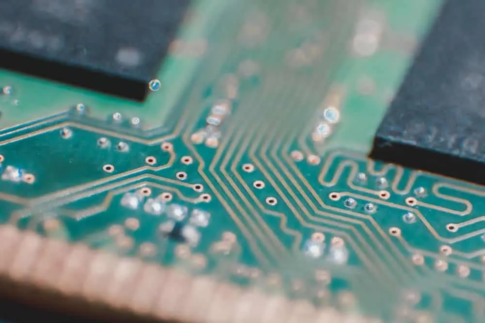
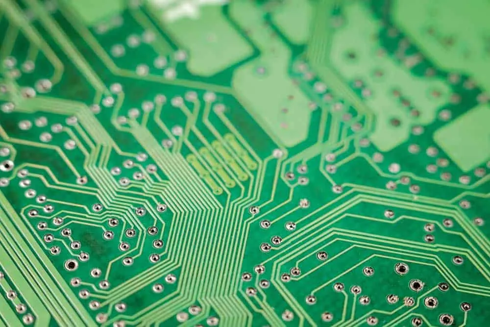
GPU PCB Layer Structure
Layer Count and Purpose
Modern GPU PCBs typically utilize 6-16 conductive layers depending on complexity and performance targets. Each layer serves specific purposes in the overall design:
| Layer Type | Purpose | Typical Position | |------------|---------|------------------| | Component Layer | Mounts GPU, memory, and surface components | Top (Layer 1) | | Ground Plane | Low-impedance current return path | Layer 2 | | Signal Layers | Route high-speed interconnections | Layers 3-6 | | Power Planes | Distribute power with high ampacity | Layers 7-8 | | Stiffening Layers | Improve structural rigidity | Layers 9-10 |
Higher layer counts enable more sophisticated routing options, better power distribution, and improved signal integrity through dedicated reference planes. Premium designs may utilize 12+ layers enabling optimal separation between sensitive signals and noisy power circuits.
Functional Sections
GPU PCBs organize components into functional sections simplifying routing and thermal management:
GPU Section: Central area hosting the graphics processor surrounded by decoupling capacitors and immediate power delivery components.
Memory Section: Memory chips arranged around the GPU with associated power and control circuitry maintaining minimal trace lengths to the GPU interface.
Power Delivery Section: VRM components grouped together enabling efficient power distribution and thermal management through dedicated heatsinking.
I/O Section: Connectors including PCIe interface, display outputs, and auxiliary power grouped along card edges for accessibility.
GPU PCB Materials
Base Materials
Most GPU PCBs utilize FR-4 fiberglass-reinforced epoxy as the base substrate. This material provides adequate thermal properties, mechanical strength, and electrical performance for mainstream applications at reasonable cost. Premium designs may incorporate specialized materials with improved dielectric properties or thermal conductivity for demanding applications.
Copper Layers
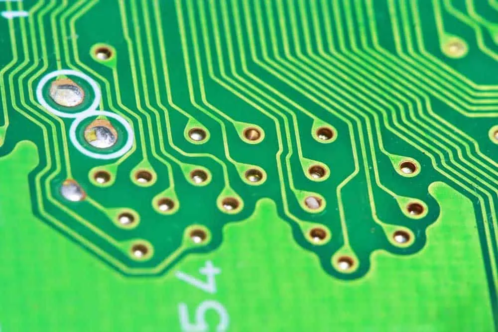
Conductive layers use copper with thickness measured in ounces per square foot. Standard 1oz copper suffices for signal layers, while power planes may use 2oz or heavier copper for lower resistance at high currents. Trace width and thickness calculations ensure adequate current capacity without excessive voltage drop or heat generation.
Surface Finishes
Solder mask protects copper traces from oxidation and prevents short circuits during assembly. Common finishes include HASL (Hot Air Solder Leveling), ENIG (Electroless Nickel Immersion Gold), and OSP (Organic Solderability Preservative), each offering different solderability, cost, and environmental characteristics.
HDI Technology
High Density Interconnect (HDI) technology enables finer trace widths and spacing critical for high-speed signal transmission. HDI allows more complex designs in smaller footprints, reducing signal latency and improving power delivery through microvias and blind/buried via structures.
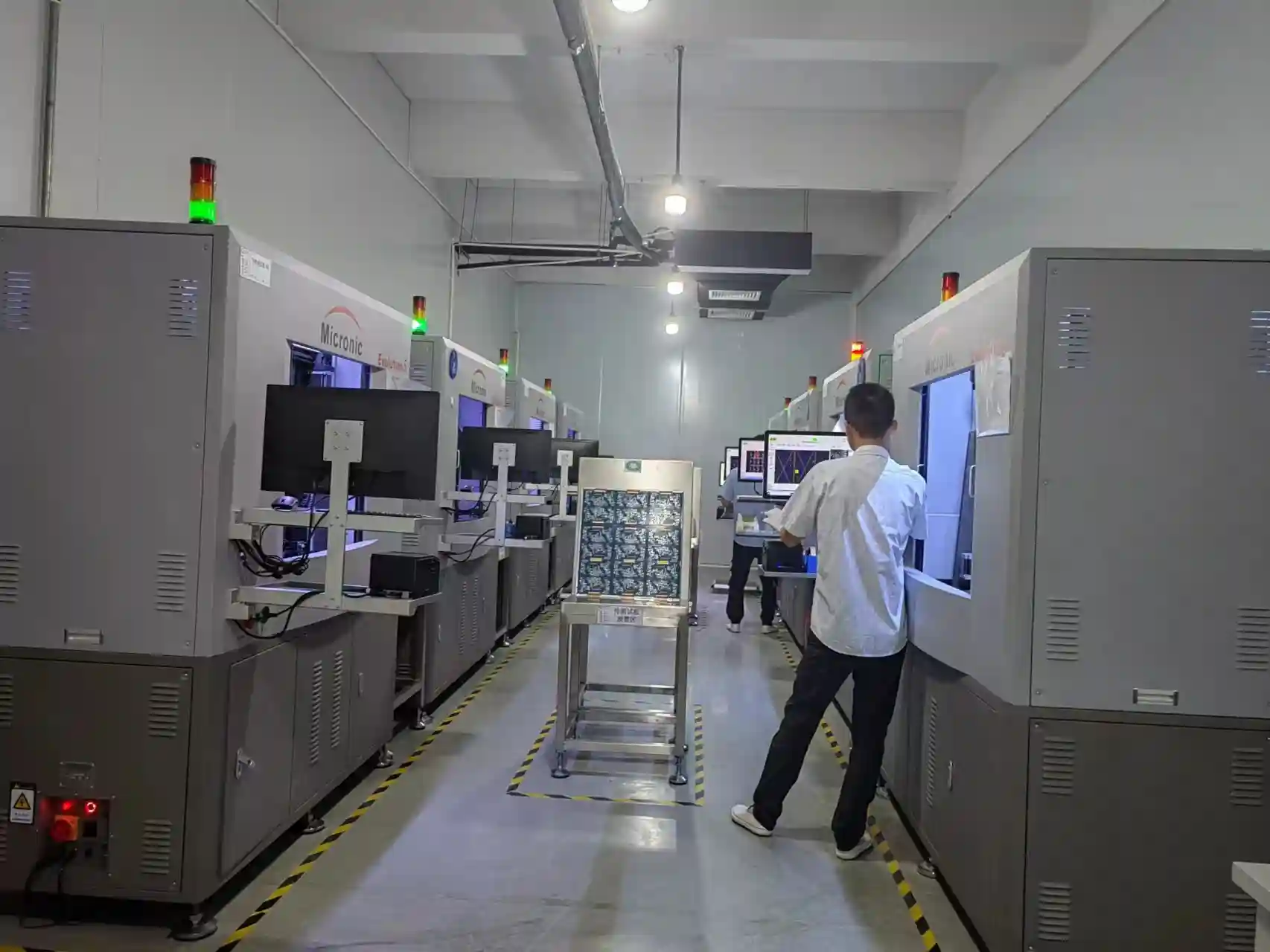
GPU PCB Production Process
Fabrication
Board fabrication begins with laminating copper layers separated by insulating substrate. Photolithographic processes define trace patterns, followed by etching to remove unwanted copper. Drilling creates via holes connecting layers, followed by plating to establish electrical connections. Multiple fabrication cycles may be required for complex multi-layer designs.
Component Population
Pick-and-place machines position surface mount components with precision measured in microns. Solder paste applied through stencils bonds components during reflow soldering, where controlled heating profiles melt solder creating permanent connections. Through-hole components and mechanical assemblies may require additional soldering operations.
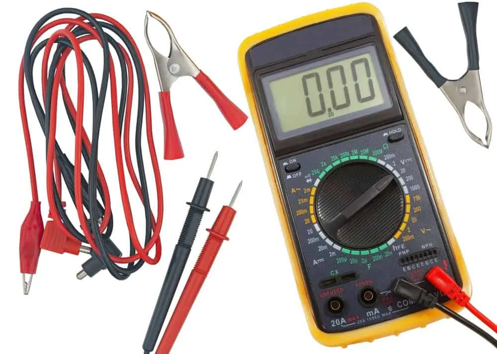
Testing and Quality Control
Automated optical inspection (AOI) verifies component placement and solder quality. Electrical testing confirms circuit continuity and identifies manufacturing defects. Functional testing validates complete board operation before integration with cooling systems and final packaging.
Revisions and Refinement
Initial production runs typically reveal design issues addressed through board revisions (Rev 1.0, 1.1, etc.). Common refinements include power delivery improvements, thermal optimizations, and component substitutions addressing availability or cost considerations.
GPU PCB Performance Tiers
Entry-Level GPU PCBs
Basic graphics cards utilize simplified PCB designs minimizing manufacturing costs:
- - 2-4 layer construction
- Basic 3+1 or 4+1 power phase designs
- Simplified filtering and protection
- Reliance on board thickness rather than additional layers for rigidity
- No backplate or minimal structural reinforcement
These designs adequately serve basic computing, light gaming, and display output needs without supporting aggressive overclocking or maximum performance extraction.
Mainstream GPU PCBs
Mid-range gaming cards balance performance and cost:
- - 6-8 layer construction
- Improved power phases (6+2 to 8+2 configurations)
- Enhanced circuit protection and filtering
- Specialized routing for critical signals
- Full backplate providing rigidity and thermal transfer
Mainstream designs enable solid gaming performance with moderate overclocking headroom suitable for enthusiast tweaking.
Enthusiast GPU PCBs
Premium graphics cards feature no-compromise PCB engineering:
- - 10-16 layer construction
- Extensive power phases (14+ common) with premium components
- Dual-sided component population maximizing density
- Elaborate routing preserving signal integrity
- Active backplates with supplemental cooling
- High-end materials including ceramics for insulation
Enthusiast PCBs enable maximum overclocking headroom, superior power delivery under extreme loads, and thermal management supporting sustained peak performance.
Impact on Graphics Card Performance
Clock Speed Stability
Careful trace routing preserves signal integrity enabling stable operation at high clock speeds. Premium designs maintain stability at frequencies that would cause crashes on lesser boards. This directly translates to higher benchmark scores and smoother gaming performance.
Power Handling Capability
Robust power delivery facilitates drawing 300W+ while maintaining voltage stability. Quality VRMs with ample thermal margin enable sustained boost clocks without thermal throttling or power limit restrictions. Overclocking potential depends heavily on power delivery headroom.
Thermal Performance
PCB design affects how effectively heat transfers to cooling solutions. Thermal via placement, copper area, and component layout all influence temperatures affecting performance and longevity. Premium designs run cooler under load despite higher power consumption.
Long-Term Reliability
Quality materials and thoughtful design ensure reliable operation through years of thermal cycling, humidity exposure, and mechanical stress. Premium components tolerate the demanding conditions inside gaming systems better than budget alternatives.
Summary
The GPU PCB transforms raw graphics processors into functional products through careful integration of mounting, power delivery, thermal management, and signal routing. Design choices directly impact performance, overclocking potential, and long-term reliability. Understanding these fundamentals helps buyers appreciate the engineering behind premium graphics cards and make informed purchasing decisions based on their specific needs.
For custom GPU PCB manufacturing or high-performance graphics card assembly, contact WellPCB for expert consultation and competitive quotes.
Frequently Asked Questions
What is the GPU die?
The GPU die or chip is the actual silicon processor containing billions of transistors for graphics calculations. This rectangular integrated circuit represents the computational heart of the graphics card, while the PCB provides the interface transforming this raw chip into a complete product.
What is a VRM on a graphics card?
VRMs (Voltage Regulator Modules) convert 12V power supply input into the lower voltages required by GPU and memory circuits. They consist of MOSFETs, chokes, and capacitors arranged in phases that share current load. Quality VRMs maintain stable voltage despite rapidly changing power demands.
What is a GPU backplate?
A backplate is a protective metal plate mounted on the PCB's rear side. It prevents board bending under heavy cooler weight, enhances cooling by providing additional thermal mass, and provides aesthetic finish. Premium backplates may include active cooling elements like thermal pads or integrated fans.
Why do premium graphics cards perform better?
Higher-end cards use specialized PCBs with more layers, premium materials, and careful layouts optimizing signal integrity, thermal dissipation, and power delivery. This enables GPU chips to sustain higher stable clock speeds while maintaining lower temperatures and better long-term reliability.
How many layers do GPU PCBs typically have?
Entry-level cards use 2-4 layers, mainstream gaming cards feature 6-8 layers, and premium enthusiast cards may have 10-16 layers. Higher layer counts enable better power distribution, improved signal integrity, and more sophisticated thermal management.
Related Articles
Continue exploring similar topics
AOI Testing Guide: PCB Automated Optical Inspection Explained
Complete guide to Automated Optical Inspection (AOI) for PCB manufacturing. Learn how AOI works, defect detection capabilities, 2D vs 3D systems, and implementation best practices.
Bed of Nails Test Fixture Guide: PCB In-Circuit Testing Explained
Complete guide to bed of nails test fixtures for PCB testing. Learn about fixture types, pogo pins, ICT procedures, and quality control applications.
Double-Sided PCB: Complete Design and Manufacturing Guide
Master double-sided PCB design with our comprehensive guide covering manufacturing processes, layout strategies, via specifications, and cost optimization tips.
Ready to bring your PCB design to life?
Get an instant quote for your custom PCB fabrication and assembly needs.
Get Instant Quote