
FR4 Thickness Guide: Standard PCB, Core & Prepreg Options
Complete guide to FR4 PCB thickness standards including core, prepreg, and copper options. Learn why 1.6mm is standard and how to select the right thickness for your design.
The thickness of an FR4 printed circuit board represents far more than a simple mechanical dimension. This critical parameter influences electrical performance, thermal behavior, manufacturing feasibility, and mechanical reliability throughout the product lifecycle. Designers who understand how various thickness components interact can make informed decisions that optimize their designs for specific application requirements while maintaining cost effectiveness and manufacturability.
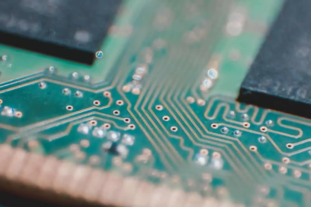
FR4 has dominated PCB manufacturing for decades due to its excellent balance of mechanical strength, electrical insulation, thermal stability, and cost efficiency. The designation FR4 indicates Flame Retardant class 4, meaning the material meets UL94V-0 standards for self-extinguishing behavior when exposed to fire. This composite material consists of woven fiberglass cloth impregnated with epoxy resin, creating a rigid substrate that provides structural support while maintaining electrical isolation between conductive copper layers.
Standard FR4 PCB Thickness Options
The PCB industry has established standardized thickness options that manufacturers optimize their processes around, resulting in cost advantages for designs using these common dimensions. Available thicknesses typically range from 0.2 millimeters for thin flexible applications through 3.2 millimeters or more for rigid high-current designs. Within this range, certain dimensions predominate due to their widespread adoption and resulting economies of scale.
The most common standard thicknesses encountered in commercial PCB manufacturing include 0.4, 0.8, 1.0, 1.2, 1.6, 2.0, and 2.4 millimeters. Each thickness serves particular application niches based on mechanical requirements, space constraints, and electrical considerations. Manufacturing tolerance typically runs plus or minus ten percent of nominal thickness, meaning a 1.6mm board may actually measure anywhere from 1.44 to 1.76 millimeters depending on the specific laminate materials and processing conditions used.
The 1.6 millimeter dimension has emerged as the de facto industry standard thickness, accounting for the majority of commercial PCB production. This dimension originated from early PCB industry practices and persists because it provides adequate mechanical rigidity for most board sizes, fits standard card edge connectors, and represents the most cost-effective option since fabricators have optimized their processes around this particular thickness. Deviating from 1.6mm typically increases cost unless production volumes justify special setup requirements.
Thinner substrates ranging from 0.4 to 1.0 millimeters suit applications where space constraints or weight limitations drive design decisions. Mobile devices, wearable electronics, and thin-form-factor products often specify these reduced thicknesses. However, thinner boards present manufacturing challenges including increased warping tendency, more difficult handling during assembly, and reduced mechanical strength that may require additional structural support in the final product.
Understanding Core Thickness
The core represents the central structural element of an FR4 PCB, consisting of fully cured fiberglass-reinforced epoxy laminate with copper foil bonded to both surfaces. Unlike prepreg material which remains partially uncured until lamination, core material arrives from suppliers in its final rigid state, providing the dimensional foundation around which the rest of the PCB stackup builds.
Standard core thicknesses available from major laminate suppliers include 0.1, 0.15, 0.2, 0.25, 0.3, 0.4, 0.5, 0.6, 0.71, 0.8, 1.0, and 1.2 millimeters. The specific dimensions available vary somewhat between manufacturers and material grades. Designers should verify availability of desired core thicknesses with their intended fabricator before finalizing designs to avoid costly material substitutions or extended lead times.
Core thickness selection directly impacts several critical PCB characteristics. Thicker cores provide greater mechanical rigidity and resistance to warping, making them preferable for larger boards or applications experiencing mechanical stress. Thinner cores enable reduced overall board thickness and can improve signal integrity in controlled impedance designs by bringing reference planes closer to signal traces. The trade-offs between mechanical and electrical considerations often drive core selection decisions.
The dielectric properties of core material, combined with its thickness, determine the impedance characteristics of signal traces routed above it. Controlled impedance designs require careful matching of trace width, dielectric thickness, and material properties to achieve target impedance values. Thinner dielectrics typically require narrower traces to maintain given impedance targets, which can limit current-carrying capacity and increase susceptibility to manufacturing variation.
Prepreg Thickness and Selection
Prepreg material serves as the bonding medium that joins multiple layers during PCB lamination. The term derives from pre-impregnated, describing fiberglass fabric that has been saturated with partially cured epoxy resin. During lamination under heat and pressure, the resin flows to fill gaps and fully cures, creating permanent bonds between adjacent layers while providing electrical insulation.
Common prepreg thicknesses include 0.05, 0.075, 0.1, 0.15, and 0.2 millimeters, though availability varies by supplier and resin system. The thickness designations typically reference the cured state after lamination, though some suppliers specify uncured dimensions that compress during processing. Designers must understand their fabricator's conventions to ensure accurate stackup calculations.
Prepreg selection involves choosing both thickness and glass style, with different weave patterns providing varying resin content and mechanical properties. Standard glass styles include 106, 1080, 2116, and 7628, each offering different characteristics. Finer glass styles with higher resin content provide better gap filling around copper features but may exhibit greater thickness variation. Coarser styles offer more consistent dimensions but require careful registration to prevent glass exposure at board edges.
Multiple prepreg sheets can combine to achieve intermediate thicknesses not available from single sheets. For example, two sheets of 0.075mm prepreg might substitute for a single 0.15mm sheet while providing different resin distribution characteristics. This flexibility enables designers to fine-tune dielectric thicknesses for impedance control while working within available material options.

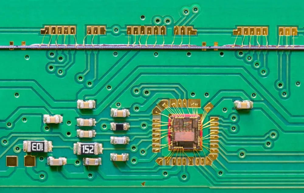
Copper Thickness Considerations
Copper thickness in PCB manufacturing is conventionally expressed in ounces per square foot, a historical unit that specifies the weight of copper covering one square foot of area. This weight-based specification translates to consistent thickness regardless of board dimensions. Standard weights and their corresponding thicknesses include half-ounce at 17.5 micrometers, one-ounce at 35 micrometers, two-ounce at 70 micrometers, three-ounce at 105 micrometers, and four-ounce at 140 micrometers.
One-ounce copper represents the most common starting weight for standard PCB manufacturing, providing adequate current-carrying capacity for most signal and low-power applications while enabling fine-pitch trace geometries. Higher copper weights increase current-carrying capacity and improve thermal dissipation but require wider traces to accommodate the thicker copper during etching processes. Very fine traces become impractical with heavy copper due to etching limitations.
Copper thickness affects the overall PCB thickness calculation, though its contribution is modest compared to dielectric layers. A typical four-layer board with one-ounce copper on all layers adds approximately 140 micrometers of copper thickness, or about nine percent of a standard 1.6mm total thickness. Heavy copper designs using two or three-ounce weights contribute proportionally more to overall dimensions.
Inner layer copper may differ from outer layer copper weights to optimize designs for specific requirements. Outer layers carrying high-current power traces might specify two-ounce copper while inner signal layers use half-ounce copper for fine-pitch routing. This mixed approach balances current-carrying requirements against routing density across different layers.
Calculating Total PCB Thickness
Total PCB thickness results from the sum of all component layers including cores, prepreg sheets, copper foils, and any surface finishes. Accurate thickness calculation requires accounting for each element's contribution, including the fact that some dimensions change during processing. Prepreg compresses during lamination, and plating processes add material to outer surfaces that must be included in final dimension estimates.
A typical four-layer stackup calculation might proceed as follows. Starting with a 0.71mm core provides the central dielectric. Adding prepreg sheets on each side, perhaps two sheets of 0.1mm each per side, contributes 0.4mm of additional dielectric. One-ounce copper on all four layers adds approximately 0.14mm. Surface finish, whether HASL, ENIG, or immersion silver, adds minimal but measurable thickness depending on the specific finish selected. The sum provides an estimated total thickness that fabricators can refine based on their specific material and process parameters.
Manufacturing tolerance must factor into any thickness-critical design. Industry standard tolerances of plus or minus ten percent mean a nominally 1.6mm board could range from 1.44 to 1.76 millimeters. Tighter tolerances are available at premium pricing for applications requiring precise mechanical fit. Designers should communicate thickness requirements clearly, specifying both nominal dimension and acceptable tolerance range.
Fabricators provide stackup tools and engineering support to help designers achieve target thicknesses using available materials. These tools model the interaction between selected cores, prepregs, and copper weights, predicting final thickness and impedance characteristics. Early engagement with fabrication partners during design development helps avoid surprises when designs reach manufacturing.
Thickness Requirements for Different PCB Types
Single-layer PCBs represent the simplest construction, with copper traces on one surface of an FR4 substrate. Standard thicknesses range from 0.4 to 1.6 millimeters depending on mechanical requirements. The absence of internal layers eliminates most complexity in thickness calculation, though copper weight and surface finish still contribute to overall dimensions.
Double-sided PCBs add copper to both surfaces with plated through-holes providing electrical connection between layers. Typical thicknesses range from 0.8 to 1.6 millimeters, with the standard 1.6mm dimension accommodating most applications. Plated hole aspect ratio limitations may require thicker substrates for designs with small vias, as very high aspect ratios become difficult to plate uniformly.
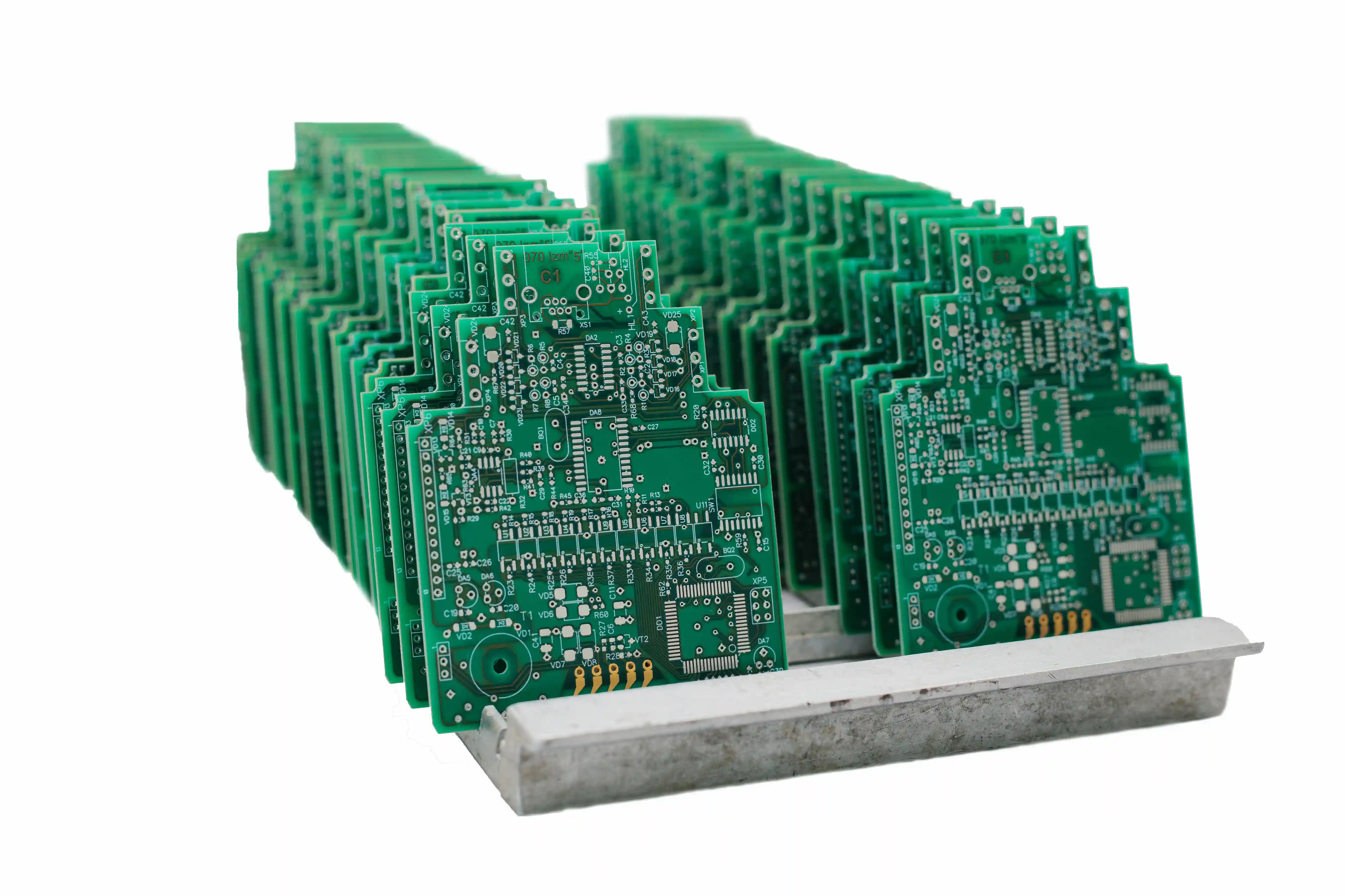
Multilayer PCBs combine multiple cores and prepreg layers to create complex stackups with four, six, eight, or more conductive layers. Total thickness depends on the number of layers and the specific materials selected for each. A four-layer board might achieve 1.0mm total thickness using thin materials, or exceed 2.0mm with standard materials plus heavy copper. Six-layer and higher designs typically exceed 1.6mm unless deliberately designed for thin construction.
High-density interconnect designs employ build-up layers with microvias laser-drilled from outer surfaces rather than mechanically drilled through-holes. These designs can achieve remarkably thin constructions while supporting high layer counts, though at significant cost premium. HDI technology enables complex routing in thin form factors essential for advanced mobile devices and miniaturized electronics.
Signal Integrity Implications
FR4 thickness directly influences signal integrity in high-speed digital designs. The dielectric thickness between signal traces and reference planes determines trace impedance, which must match driver and receiver requirements to prevent reflections that corrupt signals. Thinner dielectrics enable tighter impedance control and shorter propagation delays but require narrower traces that limit current capacity.
Controlled impedance specifications require precise matching between trace geometry and dielectric thickness. A target impedance of 50 ohms might require a 0.15mm dielectric with 0.2mm trace width, or alternatively a 0.1mm dielectric with narrower traces. Designers balance these trade-offs based on routing density requirements, current-carrying needs, and fabrication capability at their intended manufacturing partner.
Crosstalk between adjacent signal traces increases as trace spacing decreases relative to dielectric thickness. Maintaining adequate spacing relative to the distance to reference planes helps control this coupling mechanism. Thinner dielectrics bringing signals closer to reference planes can actually improve isolation by providing stronger coupling to ground rather than to adjacent traces.
Signal propagation velocity through FR4 depends on the material's dielectric constant, typically around 4.3 to 4.5 for standard FR4 grades. This relatively high dielectric constant results in propagation velocities approximately half the speed of light in vacuum. For timing-critical designs, matched trace lengths ensure signals arrive simultaneously despite physical routing differences.
Thermal Management Considerations
FR4 material exhibits relatively poor thermal conductivity compared to metals, typically around 0.25 to 0.3 watts per meter-kelvin. This limited thermal conductivity means heat generated by components dissipates primarily through copper features rather than through the dielectric material itself. Thickness affects thermal performance by determining the path length heat must travel through the board structure.
Thicker boards provide greater thermal resistance between layers, potentially trapping heat in interior regions with limited escape paths. This effect becomes significant in multilayer designs with heat-generating components whose dissipation paths pass through multiple dielectric layers. Thermal vias filled with conductive material provide low-resistance pathways through the board thickness, but their effectiveness depends on proper placement and adequate via density.
Heavy copper layers improve lateral heat spreading within the board plane, conducting heat away from concentrated sources toward larger areas where dissipation can occur. Increasing copper thickness from one ounce to two ounces roughly doubles the thermal conductivity of copper layers, significantly improving heat spreading in power electronics and other thermally demanding applications.
For extreme thermal requirements, metal-core PCB constructions insert aluminum or copper base layers that provide thermal conductivity orders of magnitude higher than FR4. These designs sacrifice some electrical design flexibility in exchange for dramatically improved thermal performance. The metal core conducts heat to enclosure surfaces or heatsinks far more effectively than FR4-based constructions can achieve.
Manufacturing Challenges at Extreme Thicknesses
Very thin PCBs below 0.4 millimeters present significant manufacturing challenges throughout the fabrication process. Handling becomes difficult as thin substrates flex and potentially crack during processing equipment transport. Registration accuracy suffers when substrates distort under mechanical stress. Warping tendency increases dramatically as thickness decreases, potentially rendering boards unassembly-able if curvature exceeds equipment tolerance.
Thick PCBs exceeding 2.4 millimeters create different challenges centered on drilling and plating operations. Mechanical drilling becomes slower and more tool-intensive as depth increases. Achieving uniform plating thickness throughout deep vias requires extended plating cycles and careful process control. Very high aspect ratio holes may exhibit thin plating at their centers that compromises reliability.
The aspect ratio between hole diameter and board thickness determines drilling and plating feasibility. Standard mechanical drilling achieves reliable results at aspect ratios up to about 10:1, meaning a 1.6mm board can reliably produce 0.16mm holes. Thicker boards or smaller holes push beyond standard capabilities, requiring either larger holes or advanced drilling and plating techniques that increase cost.
Panel utilization efficiency may suffer at non-standard thicknesses as fabricators optimize material procurement for popular dimensions. Requesting unusual thicknesses might trigger minimum order quantities or premium pricing if fabricators must special-order laminate materials. Designing to standard dimensions where application requirements permit helps control costs and improve lead times.
Conclusion
FR4 thickness selection requires balancing multiple competing considerations including mechanical strength, electrical performance, thermal management, manufacturing feasibility, and cost. The industry-standard 1.6mm thickness serves most applications well, but specific requirements may drive selection of thinner or thicker constructions. Understanding the component contributions from cores, prepreg, copper, and finishes enables accurate thickness targeting for designs with dimensional constraints.
Careful attention to stackup design during the early phases of PCB development prevents costly revisions when designs reach fabrication. Engaging with manufacturing partners early provides access to material availability information and engineering guidance that helps optimize designs for both performance and manufacturability. The investment in upfront stackup planning pays dividends through smoother fabrication and assembly experiences.
For professional PCB fabrication services with expertise in complex stackup designs and tight thickness tolerances, contact WellPCB for engineering support and competitive pricing on your FR4 circuit board requirements.
Frequently Asked Questions
What is the standard thickness for FR4 PCBs?
The industry standard FR4 PCB thickness is 1.6 millimeters, equivalent to 0.063 inches or 63 mils. This dimension accounts for the majority of commercial PCB production because it provides adequate mechanical rigidity, fits standard connectors, and represents the most cost-effective option. Manufacturers optimize their processes around this thickness, making deviations typically more expensive.
What FR4 thicknesses are available?
Standard FR4 PCB thicknesses include 0.4, 0.6, 0.8, 1.0, 1.2, 1.6, 2.0, 2.4, and 3.2 millimeters. Custom thicknesses between these standards are possible but may incur additional costs. Manufacturing tolerance typically runs plus or minus ten percent of nominal thickness, so a 1.6mm board might measure anywhere from 1.44 to 1.76 millimeters.
How do I calculate total PCB thickness?
Total PCB thickness equals the sum of all core layers, prepreg layers, copper foils, and surface finishes. A typical four-layer stackup includes one core, prepreg sheets on each side, copper on all four layers, and surface finish. Fabricators provide stackup tools that model these components and predict final thickness based on specific materials selected.
What copper thickness should I use?
One-ounce copper at 35 micrometers thickness suits most signal and low-power applications. Higher copper weights including two-ounce at 70 micrometers and three-ounce at 105 micrometers provide increased current-carrying capacity for power electronics but require wider traces. Half-ounce copper at 17.5 micrometers enables fine-pitch routing when current requirements permit.
Does PCB thickness affect impedance?
Yes, dielectric thickness between signal traces and reference planes directly determines trace impedance in controlled impedance designs. Thinner dielectrics require narrower traces to maintain target impedance values. Accurate impedance control requires careful coordination between trace geometry and stackup design, typically with fabricator engineering support to ensure manufactured results match design intent.
Related Articles
Continue exploring similar topics
AOI Testing Guide: PCB Automated Optical Inspection Explained
Complete guide to Automated Optical Inspection (AOI) for PCB manufacturing. Learn how AOI works, defect detection capabilities, 2D vs 3D systems, and implementation best practices.

Bed of Nails Test Fixture Guide: PCB In-Circuit Testing Explained
Complete guide to bed of nails test fixtures for PCB testing. Learn about fixture types, pogo pins, ICT procedures, and quality control applications.

Double-Sided PCB: Complete Design and Manufacturing Guide
Master double-sided PCB design with our comprehensive guide covering manufacturing processes, layout strategies, via specifications, and cost optimization tips.
Ready to bring your PCB design to life?
Get an instant quote for your custom PCB fabrication and assembly needs.
Get Instant Quote