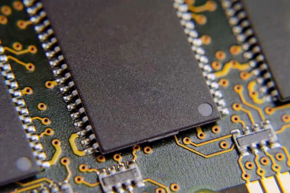
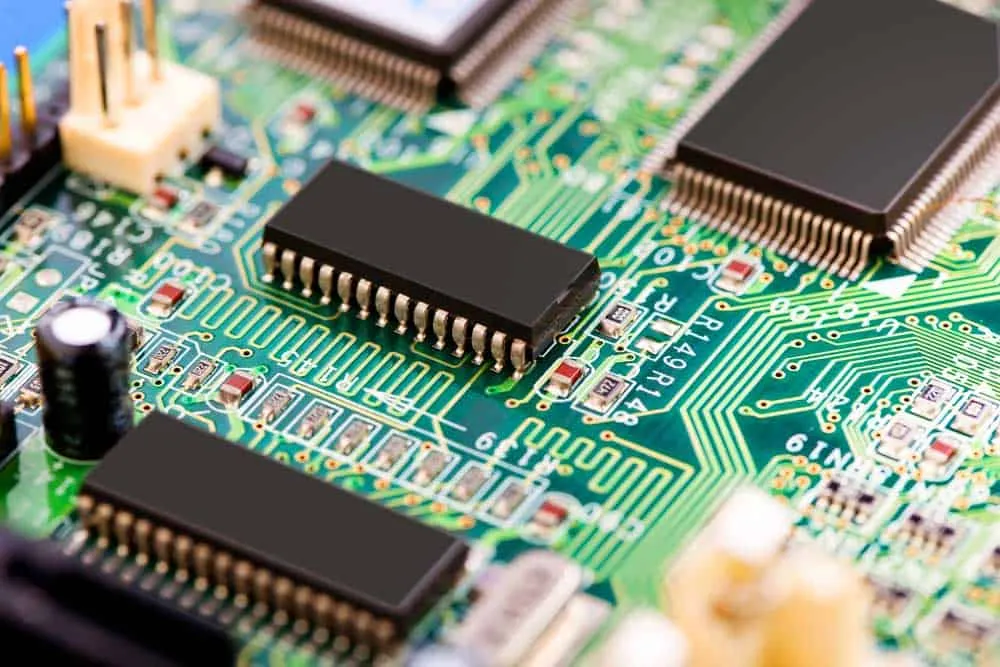
WLCSP Package
Explore WLCSP (Wafer-Level Chip Scale Packaging) technology. Learn about fan-in vs fan-out types, advantages over traditional packaging, and applications in smartphones and IoT.
We’ll look at the WLCSP package technique to learn its types, advantages, and applications.
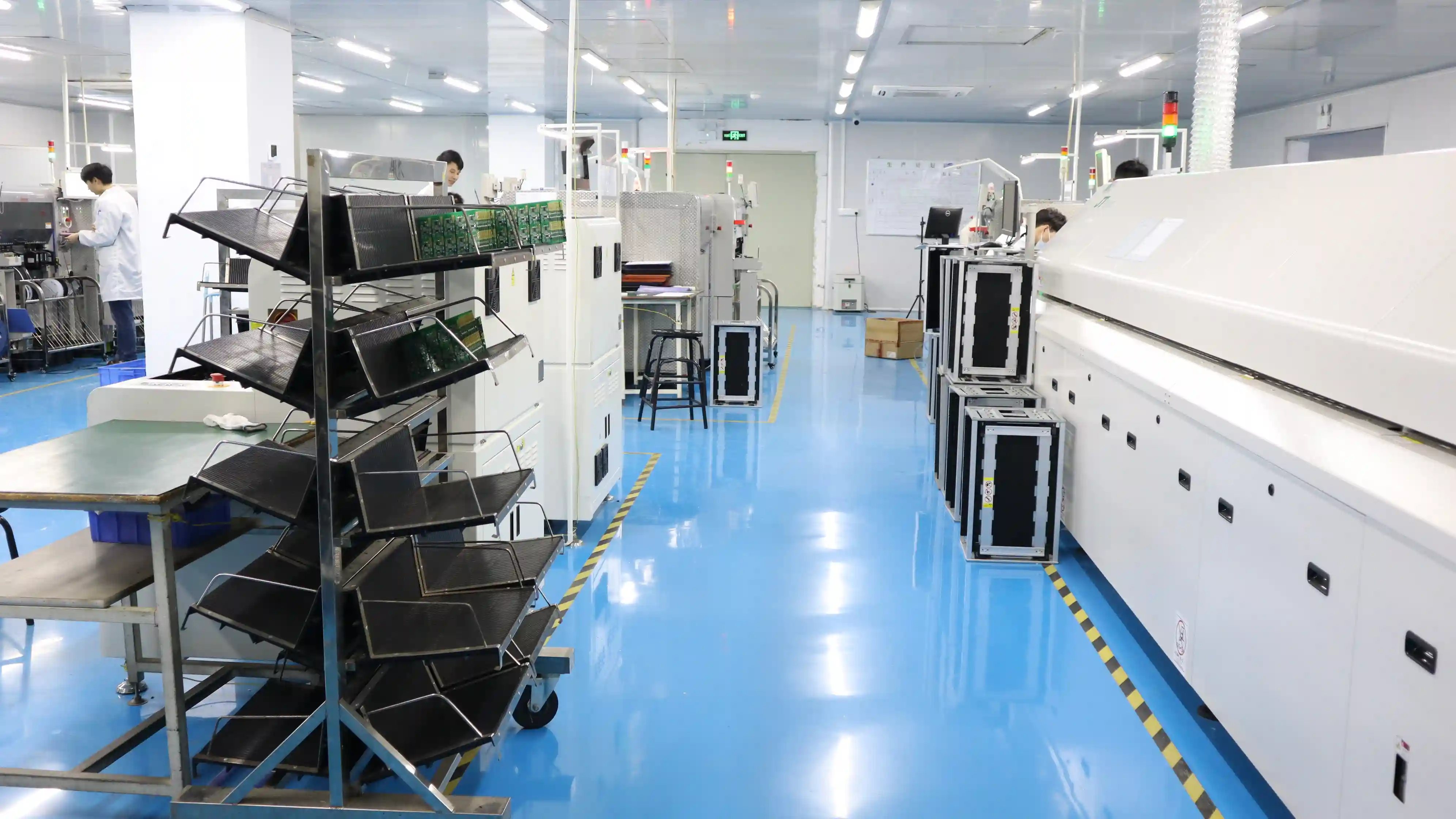
Silicon dies/chips must undergo one more processing step before PCB soldering (after wafer production). This step is the packaging.
But there are different packaging techniques, and the WLCSP package wins on several fronts. Read on to learn more!
What Is WLCSP Packaging?
WLCSP (Wafer-Level Chip Scale Packaging) is a wafer-level integrated circuit packaging technique.
The technique is a type of WLP (Wafer-Level Packaging) that involves packaging components before the wafer gets diced.
Other WLP techniques include flip chip technology, RDL (ReDistribution Layer), and TSV (Through-Silicon Via).
With the conventional packaging process, the wafer gets sliced into individual integrated circuits before component packaging.

In a nutshell, WLCSPs are bare silicon dies with an I/O pitch, redistribution layer, or interposer to rearrange the leads.
This rearrangement ensures the contact pins are large enough and have enough spacing in between for handling like ball grid arrays.
The packages differ from laminate-based CSPs and ball grid arrays because they have no interposer connections and bond wires.
Why Use WLCSP Packaging?
The WLCSP packaging technique has the following advantages.
More Compact
Generally, chip packages are broader than silicon dies.
But packing the components before wafer slicing makes it possible to create true chip-scale packages that are the same size or slightly larger than the die.
So the primary benefit of WLCSP packaging is to create compact chips to fit on boards or applications with size constraints.
And currently, the package is the tiniest in the market.
Integrated Manufacturing
Another reason is the process integrates wafer fabrication, packaging, testing, and burn-in at the wafer level to streamline the manufacturing process.
Requires No Special Soldering Equipment
WLCSP is an extension of the wafer fabrication process.
And the solder ball array pattern attached to the I/O pitch is compatible with traditional PCB assembly processes.

Better Timing, Electrical Performance, and Data Transmission
The conventional silicon die packaging process involves using wires to link the chip to the substrate in a process known as wire bonding.
Wire bonding creates connections with poor electrical performance, and the wires are not ideal for high-performance, high-frequency applications.
The situation is worse for tiny chips because the wires are longer and thinner. So such packages have timing lag and inefficient power management.
Manufacturers switched to flip-chip technology and other wafer-level packaging techniques like WLCSP to eliminate these issues.
Other advantages include:
- - Availability in different variants
- Enables horizontal or vertical chip placement
Types of Wafer-Level Packaging
Wafer-level chip scale packages fall into two primary categories, with the difference being the interposer layer.
Fan-In WLCSP
With fan-in wafer-level packaging, the die and interposer are the same size. Fan refers to the chip’s size.
So since the die and interposer sizes match, fan-in implies the package wiring, solder balls, and insulator sit directly above the chip.
This construction means the packages have the shortest dimensions.
And since the solder balls sit directly on the chip without a medium or substrate, the electrical connection is short.
But this construction results in weak chemical and physical protection because the silicon die is the package.
And usually, the chip’s coefficient of thermal expansion differs from the one on the PCB substrate.
So the solder balls connecting the two will be under immense stress after soldering the package to your PCB, creating weak solder joints.
Also, the fan-in WLCSP packaging costs can be higher than for conventional packaging if the wafer integrated circuits are few (low yield).
And if the package ball layouts are broader than the dies, it won’t be possible to create the solder ball layout to package the chip.
Lastly, you cannot use the conventional testing infrastructure to check fan-in WLCSP packages.
Fan-Out WLCSP
If you recall, fan refers to the chip size. So fan-out WLCSP packaging places the solder balls outwards compared to the silicon die, which resembles regular BGA packages.
In simpler terms, the interposer is broader than the die.
But unlike BGA, fan-out WLCSP positions the interposer directly over the silicon die.
With BGA, the interposer gets attached to the chip and reflowed using flip-chip bonding.
And compared to fan-in WLCSP, the fan-out type involves sawing the chips before packaging and placing the chips on carriers for wafer reshaping.
After that, the wafers exit the carriers and undergo wafer-level processing, followed by sawing to make the package.
With fan-in WLCSP, the wafer undergoes sawing after packaging, not in the middle of the process.
Although slightly broader than fan-in WLCSPs, the fan-out type has several advantages. For instance, you can use conventional testing equipment to check these chips.
Also, the packaging costs are lower, and you can package the dies even if the ball layout is larger than the chip.
So most device manufacturers prefer building and using these packages.
WLCSP Applications
- Smartphone image sensors, wireless, and power management functions to make them thinner
- Healthcare devices
- IoT
- I/O devices
- Bluetooth/Wi-Fi devices
- Artificial intelligence machines
- Automotive chips
- Communication devices
- High-frequency devices (RF devices)
- Specific functional devices like filters, resonators, transformers, etc.

Flip Chip vs. WLCSP
WLCSP is a variant of the flip-chip technology because it uses solder bumps instead of wire bonding for electrical connectivity. But the two packaging technologies are different.
Flip chip refers to solder bumps that rise about 50-200µm from the wafer.
And these flip-chip bumps usually have an underfill material consisting of an electrically insulating adhesive.
On the other hand, WLCSP bumps rise 200-500µm from the wafer surface, and they sit directly on the silicon die with no underfill material.
Wrap Up

When considering the fan-in type, WLCSPs are true chip-scale packages. Fan-out WLCSPs are slightly broader than the die, but they are superior to fan-in WLCSPs.
So we recommend getting the fan-out package for your project. Let’s keep engaging in the comment below and keep the conversation going. Explore our PCB assembly services for advanced chip packaging.
Related Articles
Continue exploring similar topics
Turnkey PCB Assembly
We'll discuss turnkey PCB assembly in this article. Time is money, and you will most likely waste precious time handling some tasks in the PCB assembly process.
How to Surface Mount Solder
Every electronic circuit board you interact with features hole components and surface mount devices. But do you know how to surface mount solder components?
PCB Assembly Drawing
Learn what a PCB assembly drawing includes and why it matters. Understand key elements like component placement, polarity marks, and reference designators.
Ready to bring your PCB design to life?
Get an instant quote for your custom PCB fabrication and assembly needs.
Get Instant Quote