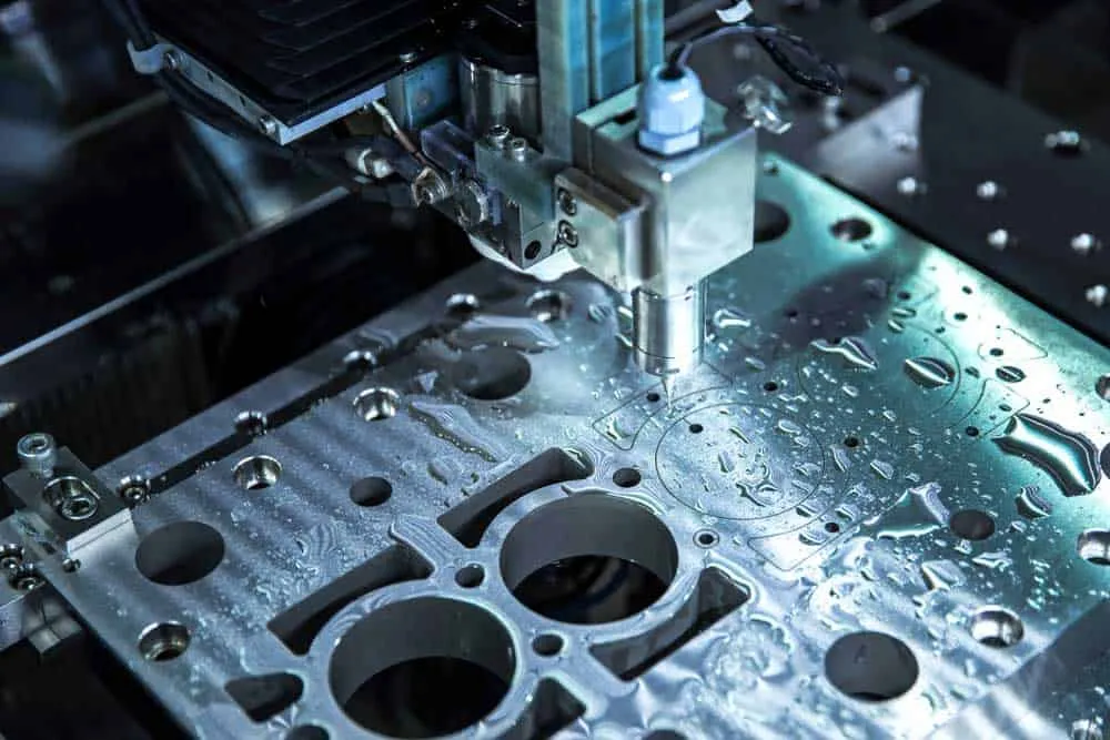
What Is a PCB Stencil? All You Need To Know
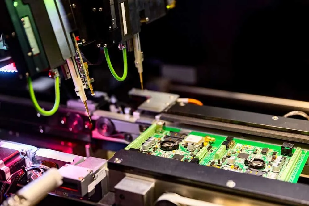
What is a PCB stencil in circuit board assembly? The process of assembling surface-mount components requires a stencil for accurate solder paste deposition.
What is a PCB stencil in circuit board assembly?
The process of assembling surface-mount components requires a stencil for accurate solder paste deposition.
Stencils also help with alignment for repeatability. So if you have multiple similar boards that need surface-mount devices, an SMT stencil will simplify the work.
Let’s dive into this topic to understand what stencils are and their design considerations.
What Is a PCB Stencil?
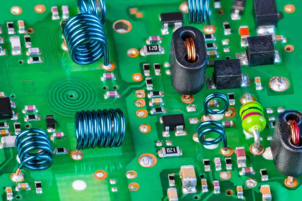
A PCB stencil is a thin sheet of material with holes to match the required SMT component soldering pads.
So the stencil design should match the PCB design. Why? Because the aperture formation will determine the SMT component layout on the board.
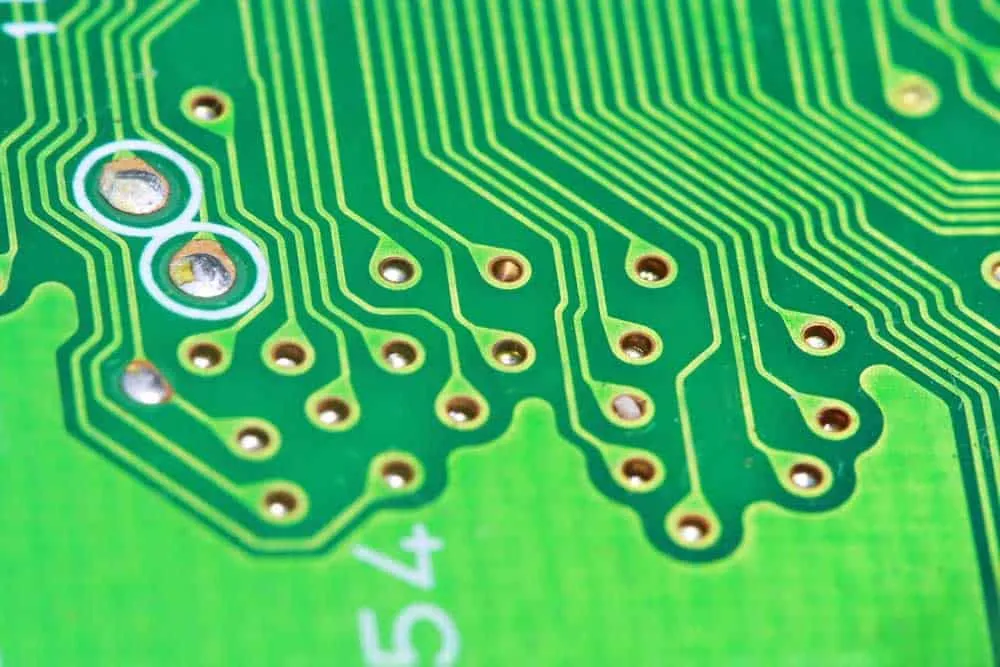
Stencils are also vital in assembling tiny surface-mount devices because they allow you to deposit appropriate solder paste quantities.
This solder paste volume control ensures solder joints provide optimal electrical connections and have the required mechanical strength.
What You Need To Make a PCB Stencil
An SMT stencil consists of four materials.
Stencil Frame
But the fixed type has the wire mesh stuck using glue. This design makes it easy to get uniform tension on the steel sheet, which usually ranges from 35-42N/cm2.
Sheet
Stencil sheets can comprise different materials, such as copper, polyester, nickel alloy, or stainless steel.
But the most common material is 301 or 304 stainless steel because it has superb mechanical properties. These properties enhance the stencil’s service life.
Mesh
A mesh fixes the stencil frame and steel sheet. And it can either be a polymer polyester or stainless steel mesh.
Stainless steel mesh types are stable and have sufficient surface tension over the short term. But they deform and lose surface tension in the long run.
So the best alternative is to use polyester meshes. The material does not deform over the long run, implying a long service life.
Glue
Types of PCB Stencils

SMT stencils come in different types that generally fall into these three categories.
Manufacturing Method
Considering the manufacturing method, you can have the following stencil types.
***Chemical Etched Stencil***
Making a stencil by chemical etching involves three steps.
The first is masking specific areas to form the stencil pattern using a photosensitive material. Next, the stencil gets exposed to UV light via a photomask.
After that, the exposed sections get etched away using a chemical solution (acid), creating a precise, high-quality cut pattern.
The process has tight tolerances, making it ideal for creating apertures for hybrid and step stencils. And it is suitable for medium to high-volume circuit board production.
***Laser Cut Stencil***
Laser cutting is a straightforward process. It involves focusing a laser beam to cut patterns in metal sheets (stencil foils).
***Electroformed Stencil***
Electroforming is an additive procedure that deposits metal material in bits via electroplating. A nickel or plastic sheet acts as the base for electroplating the metal.
Although complex, this process has high repeatability. And it can create thin stencils ranging from 2-7 mils with 0.01 mil increments.
Also, since the process does not produce burrs, you don’t have to polish the stencil before use. This smoothness reduces squeegee wear, as well.

Solder Paste Application
There are also three PCB stencil types in this category.
***Frameless Stencil***
Frameless solder paste stencils are laser-cut stencils that don’t require permanent gluing to the frame.
So you can use them with stencil tensioning systems, which are reusable stencil frames.
This type is cheaper than the framed SMT stencil and has tiny grain structures that enhance aperture-to-board solder paste transfer.
But you cannot attach this stencil permanently to the frame because it has smooth aperture walls. So you can only use it for low-volume production runs (prototyping, hand printing, etc.).
***Framed Stencil***
Like the unframed stencil, this type is a laser stencil but permanently mounted on the stencil frame using glue.
This design makes these units durable enough to withstand multiple uses. So you can use the stencils for high-volume, high-wear printing applications.
Also, the stencil features smooth and taut aperture walls that produce accurate paste prints.
***Prototype Stencil***
Prototype stencils get customized from PCB Gerber or CAD files. This construction makes the apertured sheets ideal for hand soldering because it minimizes errors.
Construction Material
The last categorization is by construction material, where you can have stainless steel or Kapton/Mylar stencils.
***Stainless Steel Stencils***
Stainless steel has superior mechanical properties than Mylar and Kapton. So it allows solder paste application with minimal errors and long-lasting use.
***Kapton/Mylar Stencils***
These laser-formed stencils are cheaper than their stainless steel counterparts, but their quality is not as good.
However, they are suitable for prototyping and deliver optimal performance when hand-soldering SMT components.
Factors To Consider When Designing, Making, or Buying PCB Stencils
Consider these four factors.
Stencil Thickness
The stencil thickness determines the amount of solder paste you’ll deposit on the board.
Excess solder paste can cause defects like bridging, while less solder paste will form weak joints.
So always use stencils with the right thickness, which depends on the aperture width.
You can use this formula.
Aspect Ratio = Aperture Width/Stencil Thickness>1.5
The lowest acceptable aspect ratio is 1.5
As for the area ratio, you can use this formula.
Area Ratio = L X W2(L+W) X T>0.66
Where:
- - R is the aspect ratio
- L is the pad length
- W is the pad width
- T is the stencil foil thickness
- The lowest acceptable area ratio is 0.66
Stencil Material
Stainless steel is the most typical stencil construction material.
But if your project needs fine-pitch devices, you might have to use nickel because it releases solder paste from the apertures more smoothly.
Aperture Design
The aperture should be narrower than the PCB pad size to avoid solder beads and bridging.
In most cases, the inner aperture wall surface should be two-thirds of the PCB pad area.
Stencil Alignment
Alignment is critical to ensuring you get the solder paste applied to the right spots.
And you need to use fiducial marks on the stencil and circuit board to achieve perfect alignment.
How To Design and Manufacture PCB Stencils
PCB stencil design and manufacturing involve these eight steps.
Determine the Solder Paste Requirements
Before creating the PCB stencil design, determine the required solder paste type and thickness. Also, find out the correct pad size and spacing.
Create the Design
With the solder paste and pad parameters determined above, the next step is to create the stencil design.
You can draw the pattern manually, but we recommend using Computer-Aided Design (CAD) software.
Determine the Stencil Material
Next, pick the most suitable stencil material, which depends on the production volume and PCB design. Common materials include copper, nickel, and stainless steel.
Pick a Manufacturing Method
The manufacturing processes include chemical etching, laser cutting, and electroforming. And the selected process depends on the material and PCB design requirements.
Add Reference Marks
Fiducial or alignment marks align the stencil and circuit board during PCB assembly. So always include these marks in the stencil design.
Inspect the Design
Check the stencil design for errors like gaps and overlaps before fabrication because these defects affect the solder paste application.
Manufacture the SMT Stencil
Laser-cut, chemical-etch, or electroformed the stencil. You might have to prepare the material if using chemical etching.
This process usually involves coating the material using photosensitive materials.
Clean and Inspect the SMT Stencil
After fabrication, clean and inspect the stencil to check for debris or defects. These can interfere with accurate solder paste application.
Wrap Up
In a nutshell, PCB stencils are perforated plates used for solder paste application on SMT assembly lines.
Although their purpose is the same, they come in different types to suit different circuit board designs and production volumes.
We hope this article has been insightful. Comment below to let us know what you think. We appreciate your feedback. Check out our PCB assembly services for professional SMT assembly.
Related Articles
Continue exploring similar topics
PCB Assembly Machine
So assemblers need high-tech PCB assembly machine to mount and weld components on the board to make the circuit function as required.
What Is First Article Inspection?
What is a first article inspection?
What is CNC Technology? Industrial Guide
Discover what CNC technology is and how computer numerical control revolutionizes manufacturing. Learn about CNC machining applications in electronics assembly and PCB production.
Ready to bring your PCB design to life?
Get an instant quote for your custom PCB fabrication and assembly needs.
Get Instant Quote