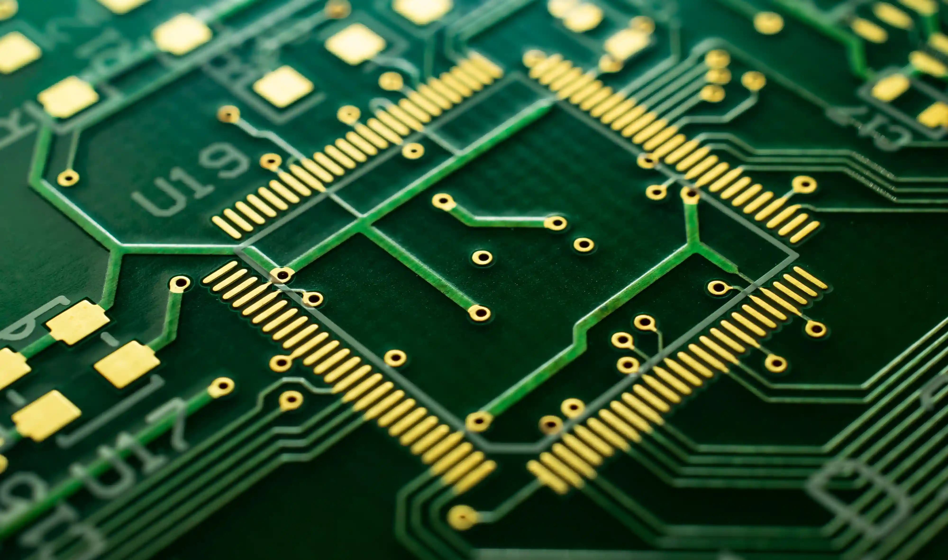
Connected Sensors, Gateways, Smart Controls, and Embedded Modules
IoT Device PCB Assembly With Firmware, RF, and Box-Build Handoff Control
PCBInsider builds IoT PCB assemblies for product teams that need more than accurate component placement. We connect SMT assembly, RF-module review, firmware identity, functional test, cable orientation, and enclosure handoff before a connected-device lot leaves the factory.
TL;DR
IoT PCBA quote control in one screen
- IoT device PCB assembly turns connected-device boards into programmed, inspected, and test-ready PCBAs.
- Best-fit programs include gateways, sensors, smart controls, wearables, and industrial monitoring devices.
- Send Gerber or ODB++, BOM, centroid, firmware notes, RF module details, enclosure drawings, and target quantity.
- PCBInsider separates RF, firmware, power, cable, and box-build risks before the first purchase order release.
SMT + THT
Mixed PCBA Route
RF Modules
Wireless Interface Review
Firmware
Program-and-Test Gate
Box Build
Connected Device Handoff
Connected Devices Fail at Interfaces, Not Only at Solder Joints
IoT device PCB assembly is a manufacturing service for connected printed circuit board assemblies used in sensors, gateways, smart controls, wearables, trackers, and embedded modules. A connected IoT product normally combines the PCBA with firmware, wireless behavior, labels, cables, power limits, and enclosure constraints, so the manufacturing plan has to cover more than placement accuracy.
Surface-mount technology is an assembly method that places components directly onto PCB pads, while through-hole assembly supports leaded connectors, terminals, and mechanically stressed parts. IoT boards often need both: surface-mount technology for dense electronics and connector-focused soldering control for field cables, antennas, batteries, displays, or enclosure-mounted interfaces.
Compact SMT Assembly
IoT boards often combine 0201 or 01005 passives, QFN sensors, fine-pitch MCUs, LEDs, antennas, and connectors in a small enclosure. We review stencil, polarity, keep-out, and AOI visibility before SMT release.
RF Module and Antenna Interface Review
Wireless modules, chip antennas, u.FL connectors, matching networks, and ground-clearance rules are checked against the PCB and enclosure path. This is where many connected products fail after a mechanically correct build.
Firmware Loading and Identity Control
Released firmware, checksum, board revision, bootloader method, MAC address, serial ID, and label rules can be tied to the lot record so each IoT PCBA ships with a known software identity.
Functional Test for Connected Behavior
Functional testing can verify boot, current draw, LEDs, buttons, sensor input, relay output, BLE or Wi-Fi response, Ethernet link, and sleep-current windows when the buyer defines practical acceptance limits.
Cable and Enclosure Handoff
IoT products rarely stop at the bare PCBA. We review board-to-cable orientation, enclosure fit, gasket or potting needs, label location, and final packing so assembly evidence survives the box-build stage.
Buyer-Readable Release Evidence
Shipment evidence can include BOM revision, firmware version, inspection route, functional-test result, serial or lot ID, deviation notes, and packing status instead of a generic final-pass statement.
Real Project Snapshot
IoT OEM Visit Expanded PCBA Scope
A European technology OEM originally purchased passive components and connectors, but its product also needed PCB assembly and box-build support. During a facility visit in China, the team reviewed the broader electronics scope instead of treating the component order as a standalone transaction.
The anonymized case-bank record keeps the concrete numbers fixed: Client visit to China facility (Oct 20-24), Service expansion from components to PCB/Assembly. That is the buying pattern this page supports: connected-device teams consolidating component, PCBA, cable, and enclosure handoffs before repeat production.
IoT PCBA Capability Scope and Limits
Service focus
IoT device PCB assembly for connected sensors, gateways, smart controls, wearables, and embedded modules
Assembly route
SMT, through-hole connectors, mixed technology, selective soldering by review, and box-build handoff
Wireless scope
BLE, Wi-Fi, LoRa, cellular module, GNSS, Ethernet, antenna, u.FL, and RF matching-network review by project
Input package
Gerber or ODB++, BOM with MPNs, centroid, assembly drawing, firmware notes, test limits, enclosure or cable drawings
Inspection path
SPI where needed, AOI, X-ray for hidden joints, microscope review, electrical screen, and functional test planning
Evidence options
Firmware version, checksum, MAC or serial ID, test result, lot traveler, deviation notes, and packing list
Best-fit stage
EVT, DVT, pilot, bridge, and repeat builds where connected-device behavior controls shipment acceptance
Out of scope
Wireless certification ownership, unreleased firmware debugging, app development, and cloud-platform validation
A microcontroller unit is the embedded processor that runs device logic, and a wireless module is a radio subassembly that connects the product to BLE, Wi-Fi, LoRa, cellular, or another network. We can assemble and test around those entities, but product-level wireless certification and cloud validation remain buyer-owned deliverables.
Standards and Test Evidence Buyers Should Ask For
IPC-A-610 is the common PCBA workmanship reference buyers use for solder joints, component orientation, cleanliness, and acceptance classes. Public background on IPC in electronics helps frame the inspection conversation, but an IoT RFQ still needs product-specific limits for current draw, boot behavior, wireless response, firmware version, and label identity.
ISO 9001:2015 is a quality-management framework for controlled procedures, records, corrective action, and traceability. It is useful context for connected-device manufacturing because a firmware checksum, serial label, or deviation note must be controlled like any other release record. The public ISO 9000 quality management overview explains the system-level idea, while the lot traveler proves what happened on a specific PCBA build.
Wireless certification should stay visible during manufacturing review. The FCC equipment authorization overview explains why RF devices need the appropriate authorization before marketing, importing, or use in the United States. For an IoT PCBA build, that means module identity, antenna path, enclosure material, firmware configuration, and label rules should not drift after the certification test article is approved.
Hommer Zhao's practical rule for IoT builds is simple: "Do not release a connected-device PCBA until the buyer knows which checks happen before enclosure work and which checks happen after final integration. A board can pass AOI and still fail in the field if the antenna, firmware, label, or cable route was not part of the traveler."
Common IoT Board Types and Release Risks
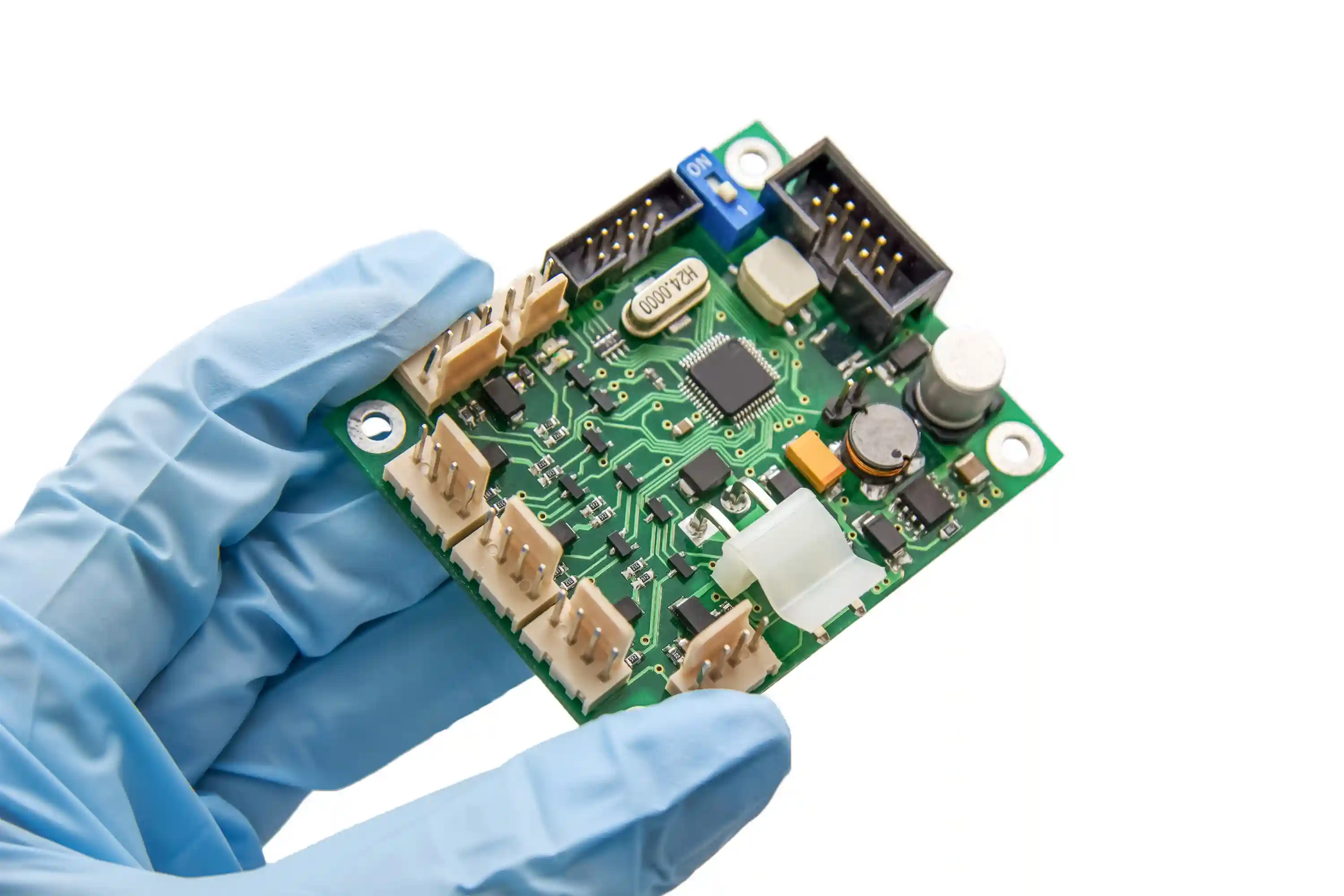
IoT device PCB assembly should separate board function from release evidence. A smart sensor, gateway, and wearable may all use SMT, but they fail for different manufacturing reasons.
| Board type | Typical electronics | Release risk to control |
|---|---|---|
| Sensor node PCBA | MCU, sensor ICs, power regulation, battery input, and wireless module | Sleep current, polarity, sensor calibration, and firmware identity |
| Gateway PCBA | Ethernet, Wi-Fi, cellular, GNSS, memory, LEDs, and external connectors | RF coexistence, connector fit, thermal load, and final functional test |
| Wearable or portable PCBA | Battery charging, BLE, LEDs, button interface, compact antennas, and flex or cable exits | ESD, fine-pitch assembly, battery safety notes, and enclosure clearance |
| Industrial IoT controller | Field I/O, relays, terminal blocks, wireless backhaul, and rugged enclosure interface | Selective soldering, surge-protection parts, coating or potting decision, and label control |
| Smart-home control board | AC/DC power, relays, wireless module, indicator LEDs, and plastic-enclosure fit | Isolation spacing, relay solder joints, firmware version, and box-build sequence |
The practical implication is that one generic "PCBA pass" label is not enough. A gateway may need Ethernet link and cellular module checks, while a battery sensor may need sleep-current measurement and label traceability. The quote should define those differences before purchasing begins.
Which Buying Path Fits Your Connected Product?
IoT buyers usually compare three sourcing paths. The right choice depends on how much risk sits beyond ordinary soldering and whether the product must ship as a programmed module or a finished enclosure-level assembly.
General PCB assembly
Board-level SMT and through-hole population
Use when the product risk is mostly solder quality and ordinary inspection.
IoT device PCB assembly
PCBA plus RF module, firmware, current, cable, and enclosure handoff controls
Use when connected behavior, battery life, antenna path, or identity records can stop shipment.
Full EMS or box build
PCBA, cable assemblies, enclosure integration, labels, final test, and packout
Use when the buyer wants a finished connected device or subassembly ready for deployment.
Choose the IoT device PCB assembly path when your RFQ includes firmware, wireless modules, MAC or serial identity, current windows, or enclosure interface risk. Choose electronics manufacturing services when the same supplier should control the finished device build rather than only the board.
IoT Device PCB Assembly Workflow
Step 1
Lock the connected-device risk map
Engineering reviews board files, BOM, RF module notes, antenna placement, firmware access, enclosure constraints, cable interfaces, quantity, and shipment evidence requirements.
Step 2
Review BOM and wireless module availability
Sourcing checks MCU, sensor, connector, memory, power, and wireless-module lines for lifecycle risk, MSL handling, approved alternates, and buyer-controlled parts.
Step 3
Build the SMT and connector route
The process route defines stencil strategy, placement, reflow, through-hole or selective soldering, ESD handling, cleaning limits, and inspection coverage.
Step 4
Program and functionally screen the PCBA
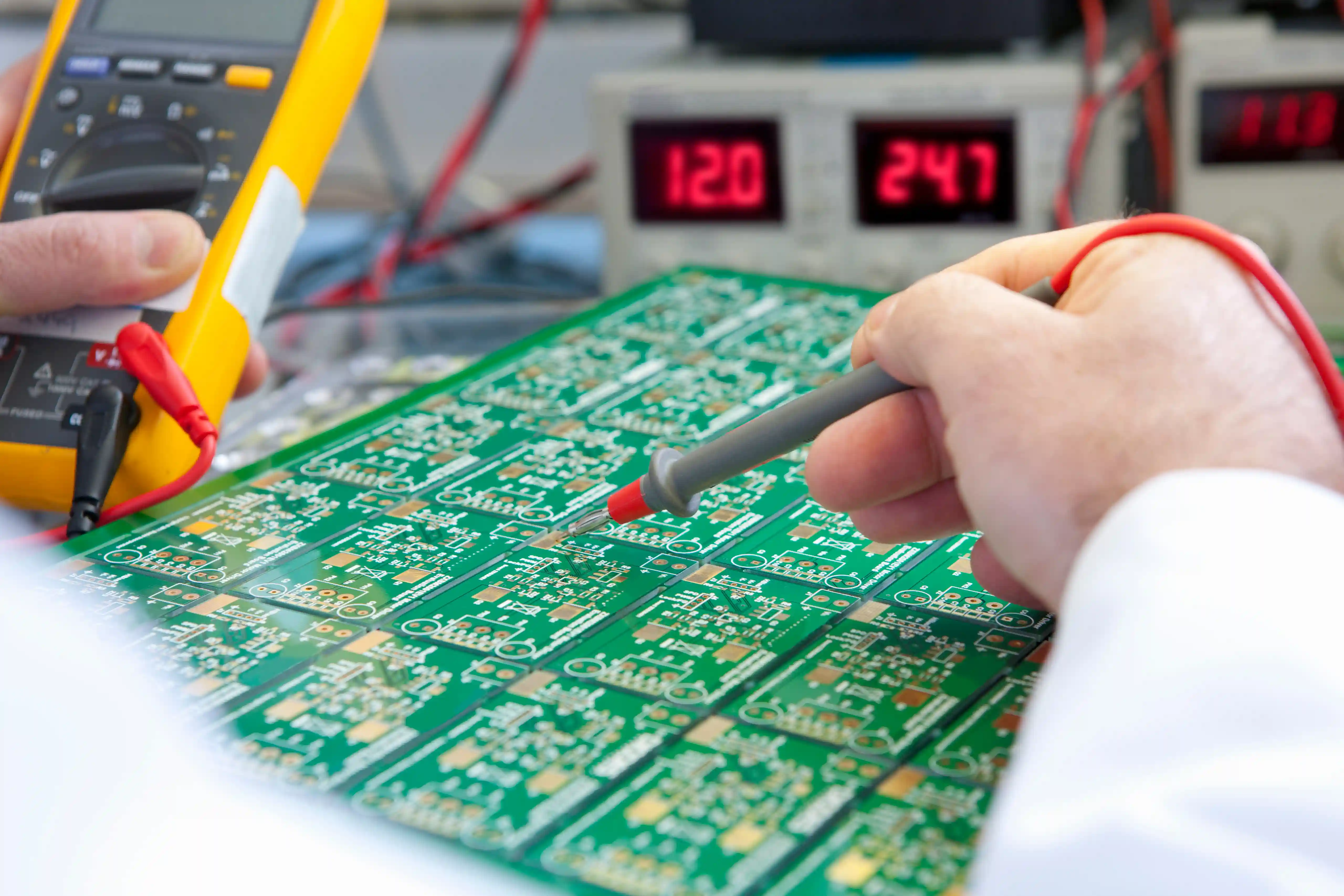
Released firmware, checksum, serial or MAC rule, boot response, current draw, I/O behavior, and communication checks are run against buyer-approved limits.
Step 5
Release box-build or shipment evidence
PCBAs move into cable, enclosure, potting, coating, labels, or final packing only after the lot record captures the agreed inspection and test evidence.
What To Send For a Useful IoT PCBA Quote
A useful IoT device PCB assembly quote needs the data that defines soldering, software identity, wireless behavior, and final integration risk. Send Gerber or ODB++, BOM, centroid, assembly drawing, firmware notes, programming method, test limits, module datasheets, antenna constraints, enclosure drawings, cable drawings, labels, target quantity, and shipment schedule.
PCBA Programming and Functional Test Release Gate
Control firmware loading, functional test, serialization, and shipment release before pilot PCBA moves into production.
Read guideMCU Component Sourcing for PCB Assembly
Manage MCU sourcing, AVL locks, firmware risk, counterfeit screening, and quote evidence before PCBA release.
Read guidePCB Assembly Supplier Consolidation
Decide when to consolidate PCB assembly, component sourcing, cables, and box-build work with one manufacturing partner.
Read guideIoT Device PCB Assembly FAQ
Answers for hardware, sourcing, and manufacturing engineers comparing IoT PCBA suppliers before releasing a connected-device RFQ package.
What files do I need for an IoT device PCB assembly quote?
Send Gerber or ODB++, BOM with manufacturer part numbers, centroid data, assembly drawing, firmware image or version notes, programming method, RF module or antenna notes, enclosure drawings, cable interface details, target quantity, and test limits. IoT device PCB assembly quotes need both board files and product-context files because a 4-layer sensor board can pass AOI but fail shipment if the antenna clearance, MAC label, or sleep-current limit is missing from the release package. Mark any IPC-A-610 class, ISO 9001 record need, or serial-number rule before pricing.
How is IoT PCBA different from standard PCB assembly?
IoT PCBA adds connected-device controls to standard SMT and through-hole assembly. The quote must cover wireless-module fit, antenna keep-out, firmware loading, serial or MAC identity, current draw, sensor response, enclosure clearance, and cable orientation. Standard PCB assembly may stop after AOI, X-ray, and electrical screening. IoT device PCB assembly usually needs a powered functional test because boot behavior, communication response, and sleep-current windows can determine whether a production lot is accepted. If FCC or CE evidence matters, freeze the module and antenna configuration before first article.
I need 500 connected sensor boards for a pilot build. Should firmware be loaded by the PCBA supplier?
Firmware should usually be loaded by the PCBA supplier when the 500-board pilot requires serial control, checksum evidence, MAC labeling, or powered functional test before shipment. Keep firmware with your engineering team only if code changes daily or the acceptance limits are not released. A practical middle path is to freeze one pilot firmware image, define the programming interface, record checksum or version ID, then let the supplier program and test each PCBA against approved limits. Ask for the pass/fail log format before the pilot lot starts.
Can PCBInsider handle IoT PCB assembly and box build together?
Yes. PCBInsider can coordinate IoT PCB assembly with cable assemblies, enclosure work, labels, firmware loading, and final functional test when the connected product needs a controlled handoff beyond the board. One case-bank example involved a European technology OEM that visited the China facility from Oct 20-24 and expanded the discussion from wiring harness parts into PCB/Assembly and box-build capability. That type of scope works best when the RFQ includes both PCBA data and mechanical drawings. Include packing, label, gasket, and cable-routing requirements with the first quote request.
What quality standards should I mention in an IoT PCBA RFQ?
Mention IPC-A-610 for finished PCBA workmanship, IPC J-STD-001 for soldered electrical and electronic assembly expectations, ISO 9001:2015 for document-control discipline, and any product-specific safety or wireless certification requirements your company owns. Standards do not define the whole IoT release. Add practical limits such as boot time, current draw, BLE or Wi-Fi response, sensor range, firmware version, label format, and whether every board needs a serial-linked test log. State the acceptance class and required evidence package clearly in the RFQ notes.
When should an IoT board use conformal coating or potting?
Use conformal coating when an IoT PCBA needs moisture, dust, or condensation protection while still allowing some rework and connector access. Use potting when the module needs stronger environmental sealing, vibration support, or tamper resistance, but accept that rework becomes harder. For outdoor sensors, battery devices, and industrial gateways, the decision should consider heat, antenna detuning risk, connector exposure, serviceability, and whether the enclosure already controls direct water entry. Define keep-out zones around antennas, switches, headers, and test pads before coating approval.
Can you certify the wireless product for FCC, CE, or carrier approval?
PCBInsider can build the IoT PCB assembly, preserve manufacturing evidence, and support test-unit preparation, but final FCC, CE, carrier, or product-level wireless certification remains the product owner's responsibility. If the design uses a pre-certified BLE, Wi-Fi, LoRa, or cellular module, the RFQ should identify the module, antenna, enclosure material, labeling rule, and allowed firmware configuration. We can help keep the assembly route consistent with the released certification test article. Any antenna, housing, firmware, or module change should trigger engineering review before production release.
Related Services
IoT device PCB assembly sits between board-level PCBA, RF-aware design, firmware testing, and finished-product integration. These pages help define the right scope before you request pricing.
PCB Assembly
Use the broad PCBA page for SMT, through-hole, BGA, inspection, sourcing, and prototype-to-production assembly scope.
Explore servicePCBA Programming and Functional Testing
Use this service when firmware loading, serial records, powered behavior, and release evidence are the main buying concerns.
Explore service5G Antenna PCB Manufacturing
Use this path when the IoT program depends on RF-aware antenna PCB stackup, materials, impedance, and assembly handoff.
Explore serviceBox Build Assembly
Use box build when the connected-device PCBA must continue into cables, enclosure integration, labels, final test, and packout.
Explore serviceNeed an IoT PCBA quote with firmware and RF risk reviewed?
Send your files, target quantity, firmware notes, wireless module details, and enclosure constraints. We'll review assembly route, sourcing risk, test limits, and box-build handoff before pricing.
Reviewed by Hommer Zhao, PCBInsider founder and technical expert. Hommer works with PCB fabrication, PCBA sourcing, cable integration, firmware-test release, and box-build programs for connected electronics buyers.