Advanced Electronic Assembly
IC Assemblies for Dense, High-Reliability Electronic Products
PCB Insider builds IC-heavy assemblies for products where package density, hidden solder joints, thermal behavior, and traceability matter more than simple placement speed. We support prototypes, NPI, and production for fine-pitch packages, module builds, and mixed-technology electronic subsystems.
0.3 mm
BGA Pitch Support
X-Ray + AOI
Inspection Coverage
Prototype to Volume
Program Range
24 Hours
Typical Quote Turnaround
What Buyers Need from an IC Assembly Partner
IC assemblies are usually won or lost on process discipline, not line-rate claims. These are the manufacturing controls we focus on when package density and hidden-joint reliability drive the risk.
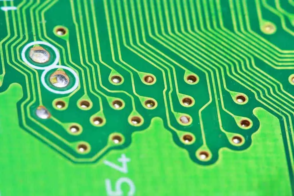
Fine-Pitch IC Placement Control
Dense package assemblies fail when paste design, placement accuracy, and thermal behavior are treated like standard SMT.
Hidden-Joint Inspection Strategy
Package types such as BGA, LGA, and bottom-terminated components require more than visual confirmation.
Package-Specific Process Windows
Thermal mass, moisture sensitivity, and pad geometry vary widely between logic devices, memory, RF parts, and power semiconductors.
Traceability for Critical Components
IC-heavy products often need lot tracking, MSL handling, and documented material control.
Module and Subsystem Integration
IC assemblies are often only one part of the delivered product.
NPI Discipline That Scales
A stable first build is not enough if the process cannot repeat.
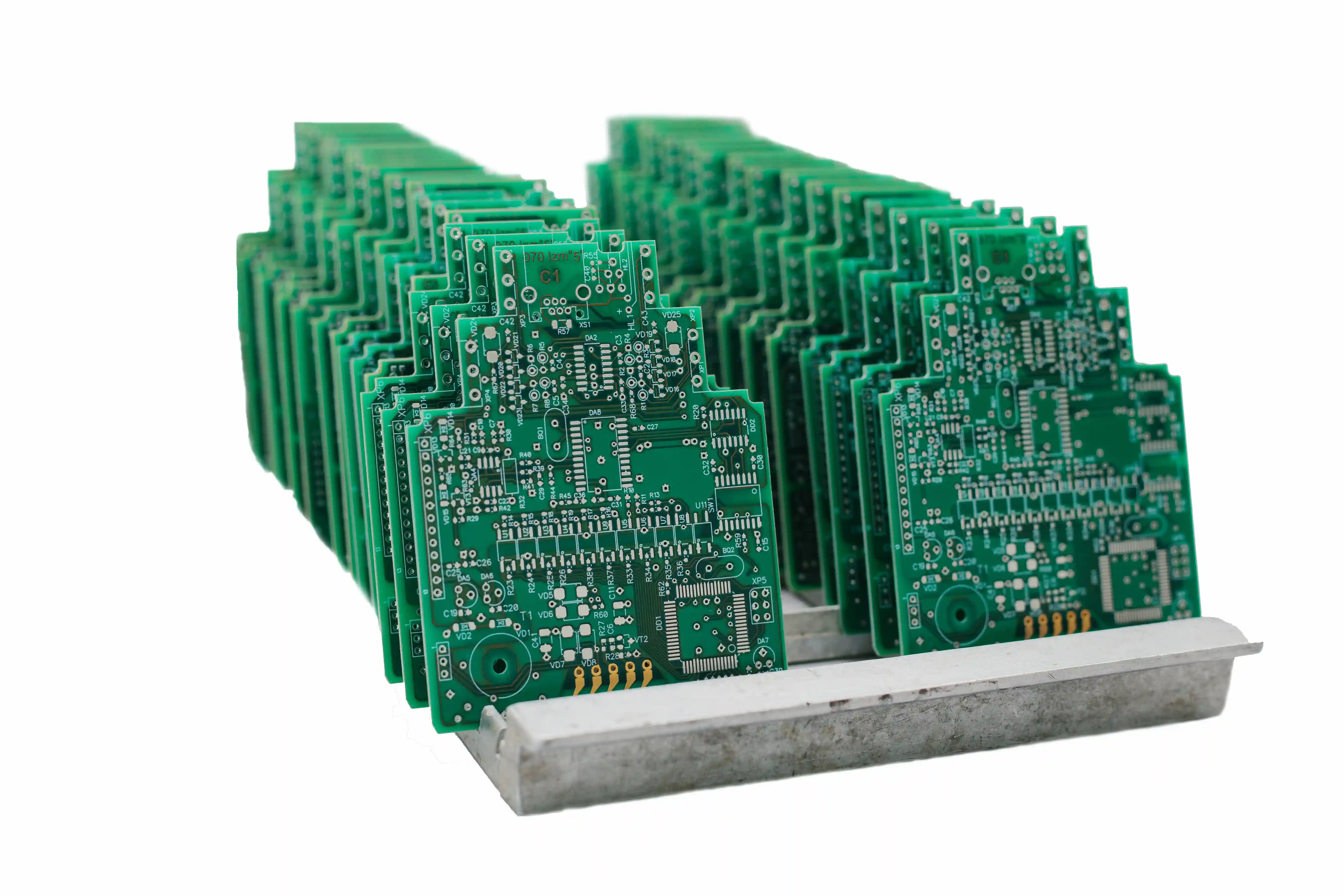
IC Assembly Capabilities
We support advanced package assembly inside a broader EMS workflow, so the project does not stop at board population. If your program also needs sourcing, shields, interconnects, or system-level integration, we can scope that into the build plan from the start.
Our engineering approach aligns with package-specific controls commonly associated with standards and practices referenced by IPC and JEDEC, especially where moisture sensitivity, land pattern behavior, and package handling directly affect assembly yield.
| Assembly Scope | IC-heavy PCBAs, modules, and subsystem assemblies |
| Common Packages | BGA, micro-BGA, QFN, DFN, LGA, QFP, CSP, SiP |
| Placement Capability | Fine-pitch SMT with package-specific setup review |
| Inspection | AOI, X-ray by requirement, microscope verification |
| Materials Control | MSL handling, baking, lot traceability options |
| Process Options | Underfill, staking, shield install, selective hand assembly |
| Build Models | Turnkey, consigned, and hybrid procurement |
| Program Types | Prototype, NPI, pilot, bridge, repeat production |
| Documentation | Build records, first article support, revision control |
| Adjacent Services | PCB fab, cable assembly, harnesses, box build |
How We Run IC Assembly Programs
1
Package Risk and Data Review
We start with land patterns, package notes, MSL exposure, thermal constraints, and any hidden-joint concerns.
2
Stencil, Paste, and Thermal Strategy
Engineering aligns stencil apertures, paste chemistry, and reflow profile targets to the package mix on the board.
3
Controlled Assembly and In-Process Verification
Boards move through placement and soldering with checkpoints matched to the package risk.
4
Test, Integration, and Release
Completed assemblies go through the defined electrical and mechanical checks, then move into cable, shielding, or box-build steps when the project requires.
Typical IC Assembly Applications
The best-fit programs are electronics where integrated circuit content drives manufacturing complexity, inspection strategy, and field-risk exposure.
Industrial Control Electronics
Processor boards, communications modules, motion-control assemblies, and power-conversion products with dense package mixes and strict uptime expectations.
Medical and Diagnostic Hardware
Compact electronics that need disciplined material control, fine-pitch assembly, and documented process repeatability for sensitive or regulated environments.
Telecom and RF Modules
IC assemblies for networking, wireless, and RF products where package density, heat, shielding, and signal integrity all affect manufacturing yield.
Embedded and Edge Computing Systems
Compute, memory, sensor, and interface assemblies that combine advanced IC content with cable or enclosure integration for deployment-ready hardware.
Advanced Package Assembly Should Not Be an Isolated Line Item
IC assemblies usually touch broader design-for-manufacturing decisions around ball grid array, flip-chip, and dense package behavior. We structure the service around those realities so your team is not forced to manage hidden risk through email threads between separate suppliers.
If the program also requires board fabrication, cable sets, shields, thermal hardware, or final box build, we can scope the entire handoff path in one manufacturing plan.
Talk to Engineering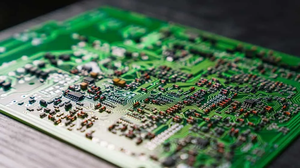
Frequently Asked Questions
What do you mean by IC assemblies?
IC assemblies are electronic builds where integrated circuits drive the manufacturing risk: fine-pitch BGAs, QFNs, LGAs, CSPs, power packages, memory devices, RF front ends, and multi-IC modules that need tighter process control than a conventional low-density PCBA.
Can you support prototype and NPI programs with advanced IC packages?
Yes. We support prototype, pilot, and bridge-production builds where package mix, underfill requirements, and inspection criteria still need refinement. Our process is designed to identify land-pattern, paste, and thermal-profile risks early before the design scales into repeat volume.
Which package types do you assemble most often?
We regularly assemble BGA, micro-BGA, QFN, DFN, LGA, QFP, SOP, TSOP, memory devices, RF modules, and application-specific mixed-technology boards that combine dense SMT with selected through-hole or cable interconnect content.
Do you provide X-ray and hidden-joint inspection?
Yes. X-ray inspection is available for hidden solder joints and void analysis on package families where AOI alone is not enough. We match the inspection plan to the package risk rather than forcing every product through the same checkpoint list.
What files do you need to quote an IC assembly project?
For the fastest quote, send Gerber or ODB++ files, a BOM with manufacturer part numbers, centroid data, assembly drawings, package notes, any underfill or staking requirements, and your preferred test criteria. If the design includes modules or sub-assembly steps, enclosure and harness drawings help as well.
Can you combine IC assembly with box build or cable integration?
Yes. Many IC-heavy products still need cable sets, shields, heat sinks, firmware loading, or final box build. We can extend beyond the dense PCB assembly step and deliver a more complete electronic subsystem when that reduces supplier handoffs.
Related Services
PCB Assembly (PCBA)
General SMT and through-hole board assembly for broader electronic builds.
EMS Provider
Single-source sourcing, assembly, integration, and production support.
Box Build Assembly
Subsystem integration when IC assemblies move beyond the bare board.
Through-Hole PCB Assembly
Mixed-technology support for connectors, power devices, and hybrid boards.