
Edge-Plated Module Manufacturing
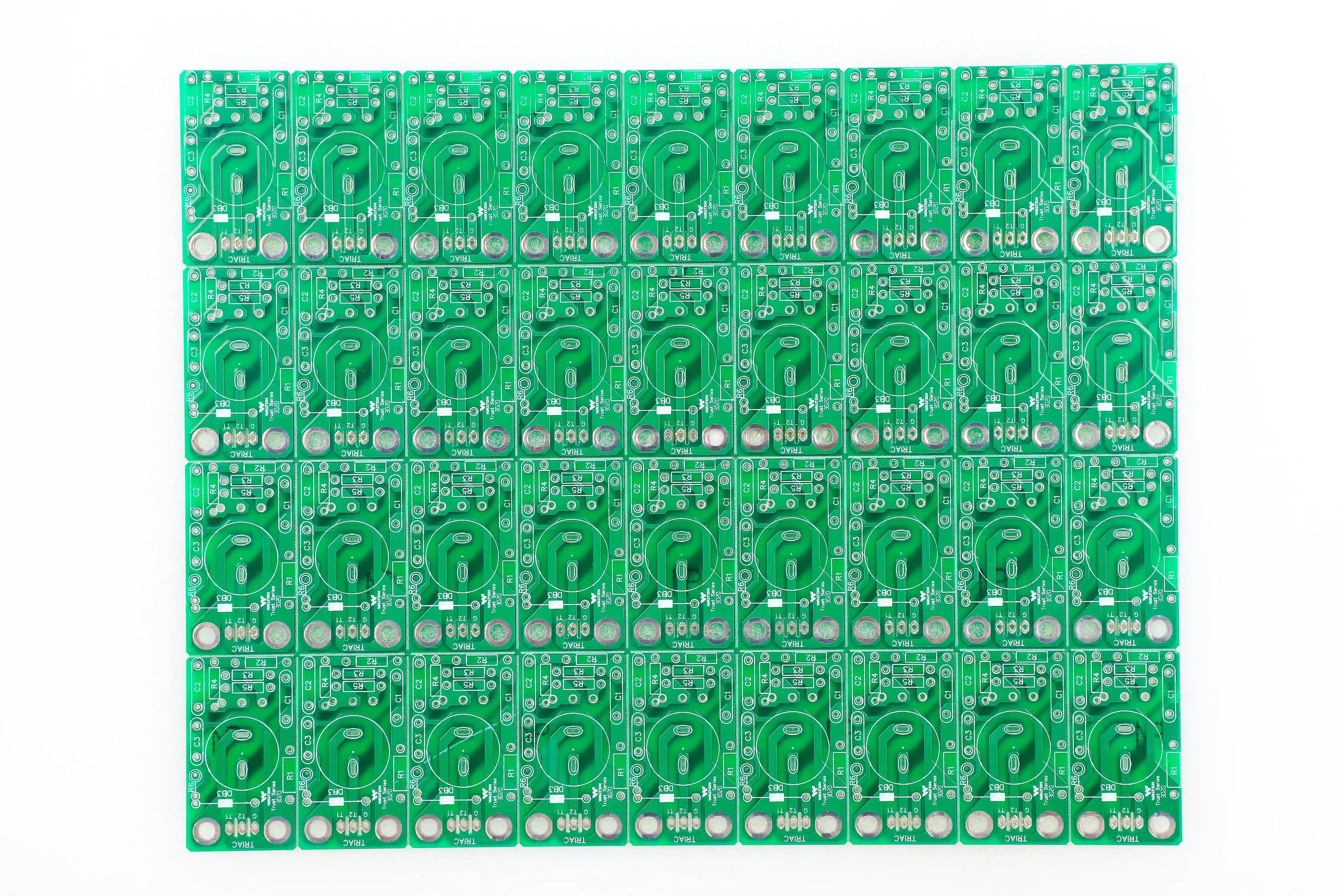
Castellated Hole PCB Module Manufacturing
PCB Insider manufactures castellated hole PCB modules for solder-down RF, IoT, sensor, and embedded electronics programs. We focus on the details that make half-hole modules work in real assembly: plating integrity, profile routing, ENIG finish, panelization, host-board footprint fit, and first-article evidence.
0.45-1.20 mm
Typical Half-Hole Diameter Range
ENIG Preferred
Solderable Module Edge Finish
100%
Electrical Test on Fabricated Panels
IPC Review
A-600, 6012, A-610, J-STD-001
Why castellated modules need assembly-aware fabrication
A castellated module is a printed circuit board designed to become part of another assembly. The half holes along the edge act as solderable terminals, so fabrication quality and host-board assembly cannot be separated. We review the module against practical surface-mount technology requirements, IPC workmanship expectations through the IPC electronics standards body, and the carrier-board soldering process before production files are treated as final.
Castellated Edge Design Review
Castellated modules fail when the board edge is treated like an ordinary outline.
Module Stackup and Material Planning
Solder-down modules often combine dense routing, RF paths, sensors, shields, or small antennas.
Panelization Built Around Half Holes
Castellated features need routing and tab strategy that protects plating at the board edge.
Finish and Solderability Control
ENIG is often selected for castellated PCB modules because flat, solderable exposed copper is critical on the edge pads.
Edge Inspection and First-Article Evidence
Finished modules are checked for burrs, copper tearing, exposed laminate, plating voids, and solder-mask registration around the edge pads.
SMT and Host-Board Assembly Support
If the module will be reflowed onto a carrier PCB, we review paste aperture assumptions, component keepout, coplanarity, and inspection access so.
Castellated PCB Module Capability Snapshot
Service focus
Castellated hole PCB module fabrication with edge-plated half holes
Best-fit modules
RF modules, IoT modules, sensor boards, embedded compute, power submodules, evaluation boards
Typical hole diameter
0.45-1.20 mm depending on pitch, board thickness, and solder joint target
Typical pitch review
1.0 mm and above is more forgiving; tighter pitch requires DFM review before quote lock
Board thickness
0.6-2.4 mm common range, with thinner modules reviewed for handling and warpage
Surface finish
ENIG preferred for flat solderable edges; other finishes by application review
Quality controls
Electrical test, visual edge inspection, dimensional check, and first-article review for NPI
Assembly handoff
Stencil, paste, reflow, AOI, and host-board footprint review available with SMT assembly
Documentation
Gerber or ODB++, drill files, fab drawing, BOM if populated, panel notes, and carrier-board context
Commercial path
Prototype modules, NPI validation, pilot builds, and repeat production after DFM signoff
Buyer Priorities
Finished edge quality
The exposed half holes are the solder joints. Burrs, lifted copper, rough routing, and inconsistent plating can make a module hard to solder even.
Host-board footprint match
A castellated module should be reviewed with the carrier PCB footprint, paste layer, and reflow process.
Panel strategy before routing
Half-hole panels need a routing sequence that preserves copper at the edge.
Clear RFQ release data
The fastest quotes include the board outline, drill table, castellated-hole callouts, surface finish, layer stackup, and intended host assembly process.
Standard castellated module workflow
For a representative 20 mm by 28 mm wireless sensor module with thirty-six 0.8 mm edge holes, the most valuable factory review is usually not the netlist. It is the half-hole profile, panel tab position, and host-board soldering plan. That is the review logic behind the workflow below.
Step 1
Review module intent and host-board context
We start with the Gerber or ODB++ package, fab drawing, drill file, target finish, quantity, and any carrier-board footprint information.
Step 2
Check half-hole geometry and edge clearance
Engineering checks hole size, pitch, annular ring, copper-to-edge clearance, solder mask clearance, and routing tolerance.
Step 3
Plan panel, plating, and profile sequence
The panel plan is selected to protect plated holes through routing and final separation.
Step 4
Fabricate, inspect, and electrically test
After drilling, plating, imaging, finish, and profile routing, boards receive electrical test and edge inspection.
Step 5
Support assembly or ship finished modules
Bare modules can ship after inspection, or move into SMT population and carrier-board assembly.
Practical release criteria for solder-down modules
Castellated holes should be defined as a controlled feature in the fabrication notes, not left as an implied board edge. We recommend tying the module drawing to IPC-6012 fabrication expectations, IPC-A-600 acceptance language for bare boards, IPC-A-610 expectations for the final assembly, and J-STD-001 soldering process requirements when the module is attached to the carrier PCB.
Best-fit programs
Wireless modules, sensor boards, small embedded controllers, power daughtercards, RF front-end boards, and design-for-test modules that must solder cleanly to a larger PCB.
Quote detail that prevents rework
Include the intended half-hole diameter, carrier-board pad dimensions, module thickness, finish, panel constraints, and whether the module will be shipped bare or populated.
Castellated Hole PCB Module FAQ
What is a castellated hole PCB module?
A castellated hole PCB module uses plated holes placed along the board edge and routed through the centerline, leaving solderable half holes. The module can then be soldered onto a larger carrier PCB like a surface-mount component.
What files do you need to quote castellated PCB modules?
Send Gerber or ODB++ files, NC drill data, a fab drawing with castellated-hole callouts, surface finish, board thickness, quantity, and any host-board footprint or assembly notes. If the module is populated, include the BOM and pick-and-place file as well.
Which surface finish works best for castellated holes?
ENIG is commonly preferred because it provides a flat, solderable finish on the exposed edge pads. Other finishes may work, but they should be reviewed against solderability, shelf life, module pitch, and host-board reflow requirements.
Can castellated modules be assembled by standard SMT reflow?
Yes, many castellated modules are designed to be reflowed onto a carrier board. The host footprint, paste aperture, module coplanarity, thermal mass, and inspection access all need review so the solder fillets form consistently along the half holes.
What makes castellated PCB fabrication different from normal PCB routing?
The board profile cuts through plated holes, so the routing sequence and panel support directly affect solderability. Ordinary outline routing can tear copper or leave burrs if the half-hole feature is not planned as a controlled manufacturing step.
Can you support RF or antenna modules with castellated edges?
Yes. RF and wireless modules are common use cases, but they need stackup, grounding, controlled impedance, keepout, and carrier-board launch details reviewed together. For RF modules, we recommend sharing the host-board constraints early rather than quoting the module alone.
Related Services
Use this page when the buying issue is the castellated module edge itself. Move to the related services below when the RFQ expands into full board fabrication, stencil planning, or assembled modules.
PCB Manufacturing
Use this for broader bare-board fabrication, stackup, finish, and electrical-test support.
Explore serviceSMT Assembly Services
Move here when the module needs component placement, reflow, AOI, and production assembly control.
Explore servicePCB Stencil Service
Useful when the castellated module will be soldered onto a host PCB and paste control matters.
Explore serviceQuick Turn PCB Assembly
For urgent prototype and NPI module builds where schedule risk must be managed tightly.
Explore serviceNeed a castellated module that solders cleanly?
Send the PCB files, drill table, fab notes, and host-board context. We'll review the half-hole geometry, finish, panel plan, and assembly risks before quoting production.
Author and Quality Context
Written by Hommer Zhao, Founder & Technical Expert at PCB Insider. PCB Insider supports PCB fabrication, SMT assembly, cable assembly, and box build programs for OEM buyers that need ISO 9001-oriented documentation, IPC workmanship review, and practical DFM feedback before production release.