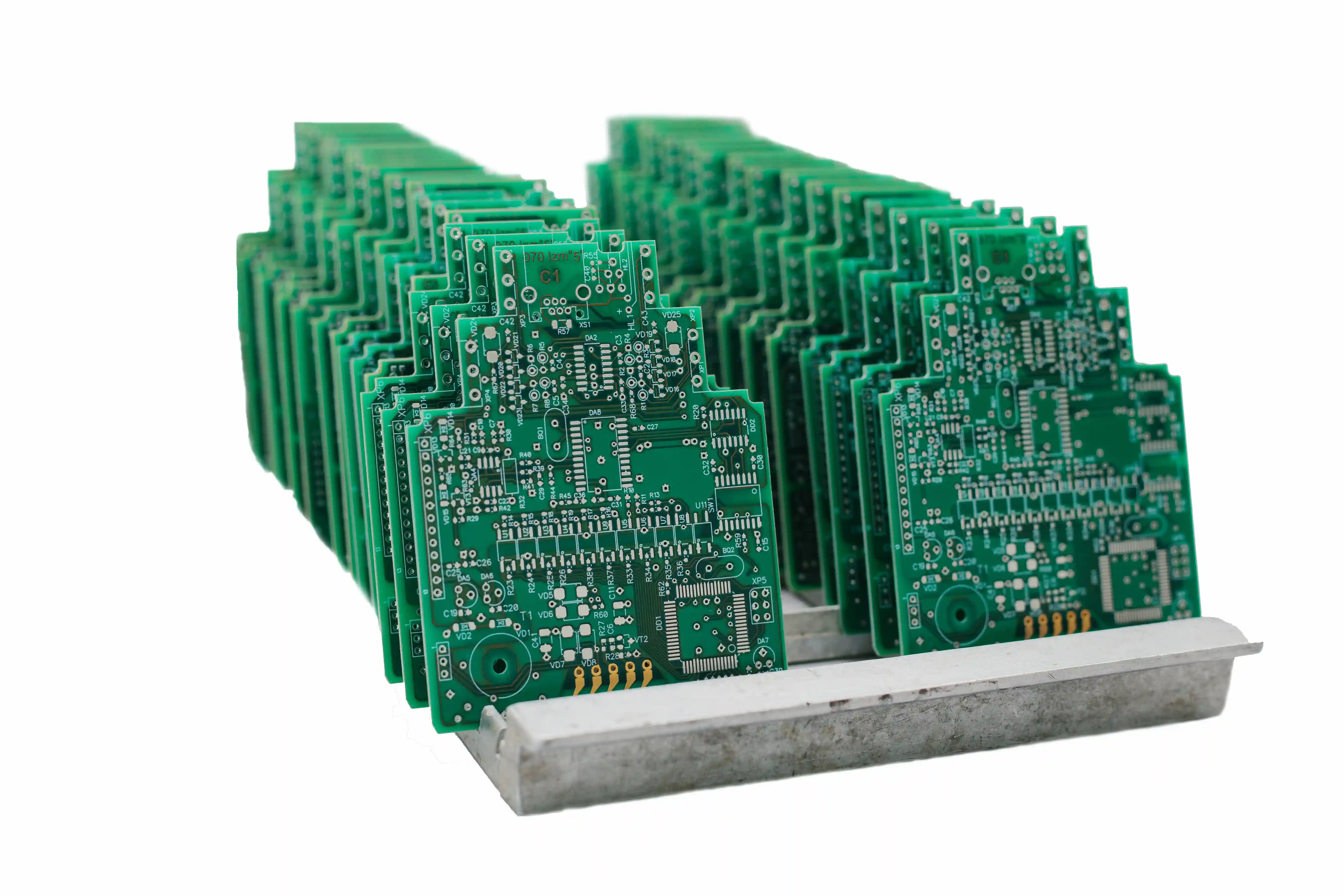
Heavy Copper PCB Service
4 Oz Copper PCB Fabrication for High-Current Hardware
PCB Insider supports 4 oz copper PCB fabrication for power electronics, industrial controls, battery systems, and other builds where standard copper no longer gives enough current margin, thermal stability, or routing efficiency.
Buyers looking for heavy copper capability usually do not need a generic board house. They need a manufacturer that can review etch limits, plating behavior, solderability, and assembly impact before release. That is the job this service is built to do.
4 oz Copper FocusDFM Before ReleaseAssembly-Ready Review
4 oz
Heavy Copper Positioning
4 oz
Finished Copper Focus
140 um
Nominal Copper Thickness
High Current
Power Board Positioning
DFM First
Release Discipline
What 4 Oz Copper Really Changes
A 4 oz copper PCB is not simply a standard board with a thicker conductor. It changes the manufacturable feature window, thermal behavior, drilling margin, plating strategy, and soldering response of the assembly. That is why heavy-copper work needs a different release mindset from ordinary quick-turn FR-4.
Copper weight is commonly referenced by ounces per square foot. In practical board terms, 4 oz copper is about 140 um thick, which is far beyond the default assumption used for many everyday PCB layouts. The underlying copper-thickness concept is summarized well in Copper in printed circuit boards .
Heavy copper is often paired with design rules from standards families buyers already know, especially IPC frameworks used to organize fabrication and assembly expectations. For broader background, see IPC (electronics) and Printed circuit board.
The manufacturing objective is straightforward: use thick copper where it meaningfully improves current carrying capacity, thermal margin, or connector interfacing, while keeping the board manufacturable and practical for downstream assembly.
Where 4 Oz Copper Fits Best
Power Conversion and Charging Hardware
AC-DC, DC-DC, inverter, charger, and battery interface boards often need 4 oz copper when bus currents or peak loads push standard copper beyond.
Industrial Motor and Drive Electronics
Heavy copper helps preserve routing width, connector landing space, and thermal margin in servo drives, pump controls, and industrial power distribution.
Battery Management and Energy Storage
BMS backplanes, protection circuits, and power interface modules frequently use 4 oz copper to keep losses down and maintain stability.
Rugged Mixed-Technology Boards
Some products need heavy current paths plus logic, sensing, and communications on the same PCB.
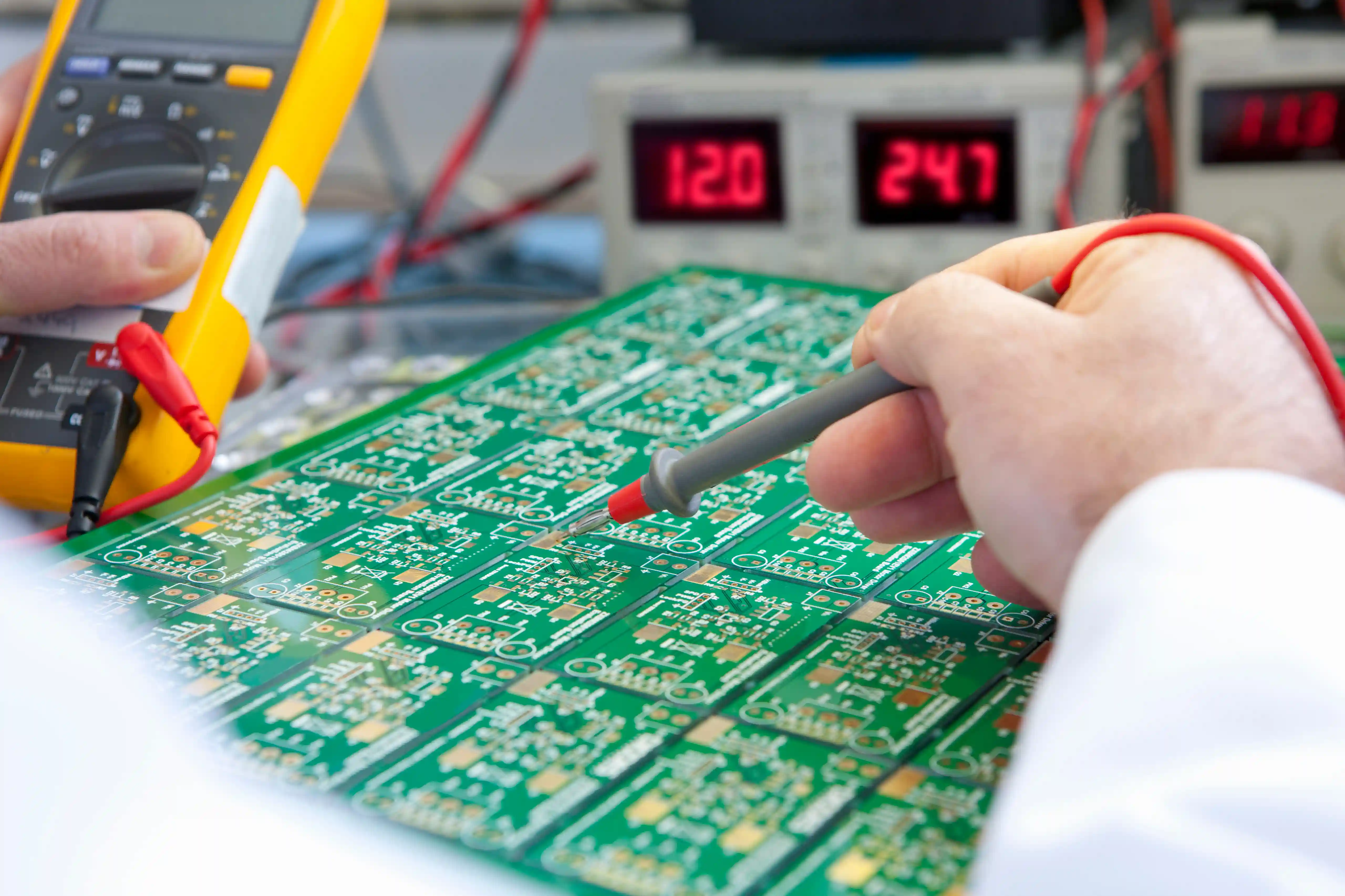
Heavy Copper Still Needs Test Discipline
High-current boards are rarely forgiving when a fabrication defect slips through. Electrical verification and inspection remain part of the release discipline, especially when the PCB is feeding expensive power components or system-level build stages.
What Buyers Need from a Heavy Copper PCB Supplier
The challenge is not finding a supplier willing to say yes to heavy copper. The challenge is finding one that understands how thick copper changes fabrication yield and downstream assembly.
Built for Real Current Carrying Loads
4 oz copper is typically selected when 1 oz or 2 oz copper forces traces to become too wide, temperature rise runs too high, or reliability margins look.
Thermal Margin Without Guesswork
Heavy copper improves current capacity, but it also changes heat spreading, pad heating, and soldering behavior.
Manufacturability Tuned for Thick Copper
Trace geometry, etch compensation, annular ring, hole wall plating, and copper balance all behave differently on a 4 oz stackup.
Power, Control, and Mixed-Function Boards
Many 4 oz projects combine high-current paths with control logic, sensing, connectors, or thermal interfaces.
Assembly-Ready Review
Heavy copper affects stencil strategy, reflow behavior, hand-solder access, and through-hole fill.
Risk Managed for Repeatability
The goal is not just one successful lot. It is a repeatable process window for prototypes, pilot runs, and production where copper thickness, drilling.
4 Oz Copper Capability Snapshot
These ranges reflect how we frame 4 oz copper fabrication in a commercial quoting and DFM discussion. The final window depends on feature geometry, copper distribution, and assembly intent.
| Service Focus | 4 oz copper PCB fabrication for high-current and thermally demanding builds |
|---|---|
| Copper Weight | 4 oz outer-layer focus; other constructions by engineering review |
| Nominal Thickness | Approx. 140 um copper for 4 oz constructions |
| Typical Layer Mix | 2-8 layers depending on current paths and control requirements |
| Common Materials | FR-4, high-Tg FR-4, selected industrial laminates |
| Min. Trace / Space | Reviewed case by case because etch compensation increases with heavy copper |
| Mechanical Drilling | Sized to maintain annular ring and plating reliability under heavy copper conditions |
| Surface Finish | ENIG, lead-free HASL, or OSP based on assembly and cost targets |
| Applications | Power supplies, motor drives, battery systems, industrial controls, LED power stages |
| Inspection | Electrical test plus fabrication inspection aligned to the released drawing package |
| Volume Fit | Prototype, NPI, pilot, and repeat production |
| Quote Inputs | Gerber or ODB++, drill, stackup, copper weight, quantity, and true current profile |

Why DFM Matters More on 4 Oz Boards
Heavy copper boards fail expensively when manufacturability is treated as an afterthought. Early review prevents unrealistic feature expectations, protects schedule, and keeps the board compatible with the assembly method planned after fabrication.
Our 4 Oz Copper Fabrication Process
The workflow is designed to front-load engineering judgment, not push risk deeper into the factory.
1
File Intake and Current Path Review
We review fabrication files, copper callouts, layer intent, current paths, thermal targets, board thickness, and quantity.
2
Heavy-Copper DFM Signoff
Engineering checks etch compensation, spacing, pad definition, annular ring margin, drill strategy, and copper distribution.
3
Fabrication with Copper and Plating Control
Once approved, the job moves through tooling, imaging, plating, etching, solder mask, finish, and profiling with the stackup window set for heavy copper.
4
Inspection, Packaging, and PCBA Handoff
Boards are electrically verified, inspected against the released package, and packed according to whether they are shipping as bare boards or moving.
Design Considerations Before You Release the Gerbers
Most heavy-copper problems are easier to solve before quote release than after CAM or assembly feedback.
Etch Compensation Increases with Copper Weight
As copper gets thicker, sidewall shape and feature definition become less forgiving.
Thermal Relief Strategy Matters
Pads tied into 4 oz copper can become difficult to solder if thermal spokes and copper balancing are not considered early.
Hole and Plating Details Need Attention
Heavy external copper changes how drilled holes, annular rings, and plated structures behave.
Not Every Net Needs 4 Oz Copper
A good heavy-copper board uses 4 oz where it solves a real electrical or thermal problem.
4 Oz Copper PCB FAQs
Common questions from engineering and sourcing teams evaluating heavy copper fabrication.
When should I choose 4 oz copper instead of 2 oz copper?
Choose 4 oz copper when the required trace width, current density, or temperature rise target cannot be met comfortably with 2 oz copper, or when surge and reliability margins justify the thicker conductor. The right decision depends on actual current profile, copper geometry, and cooling conditions rather than a generic rule.
How thick is 4 oz copper on a PCB?
A 4 oz copper weight corresponds to roughly 140 um of copper thickness. That is a useful starting reference, but the finished construction still needs engineering review because plating, stackup, and fabrication tolerances affect the final result.
Are 4 oz copper PCBs harder to assemble?
They can be. Heavy copper changes heat flow during soldering, which can affect stencil design, hand-solder effort, and through-hole fill. That is why we review assembly constraints before fabrication instead of treating heavy copper as only a fab issue.
What files do you need for a 4 oz copper PCB quote?
We need Gerber or ODB++ data, drill files, stackup intent, copper weight by layer, board thickness, quantity, surface finish preference, and any notes about true operating current or thermal requirements. Those details reduce quote revisions and DFM delays.
Can you help if my design mixes high-current copper with control circuitry?
Yes. That is a common reason to involve a manufacturing-focused review. Mixed-function boards often need tradeoffs between copper weight, spacing, solderability, layer allocation, and cost, and those tradeoffs are easier to manage before the board is released.
Related Manufacturing Resources
Review adjacent services and tools before releasing your heavy-copper board package.
PCB Manufacturing
General fabrication support from standard FR-4 through specialized constructions.
PCB Assembly
SMT and mixed-technology assembly for boards that move directly into build.
Instant PCB Quote
Send files quickly when you need a manufacturing decision on copper-heavy boards.
Copper Weight Calculator
Use the calculator to sanity-check thickness conversions and planning assumptions.
Current Density Calculator
Estimate current-loading implications before the board package is released.
IPC-2221 Overview
Review the broader PCB design standard context behind fabrication constraints.
Need a 4 Oz Copper PCB Quote That Reflects the Real Build?
Send the fabrication package with current targets, copper weight, and assembly intent. We will review the job as a manufacturable heavy-copper project rather than price it like a standard board.