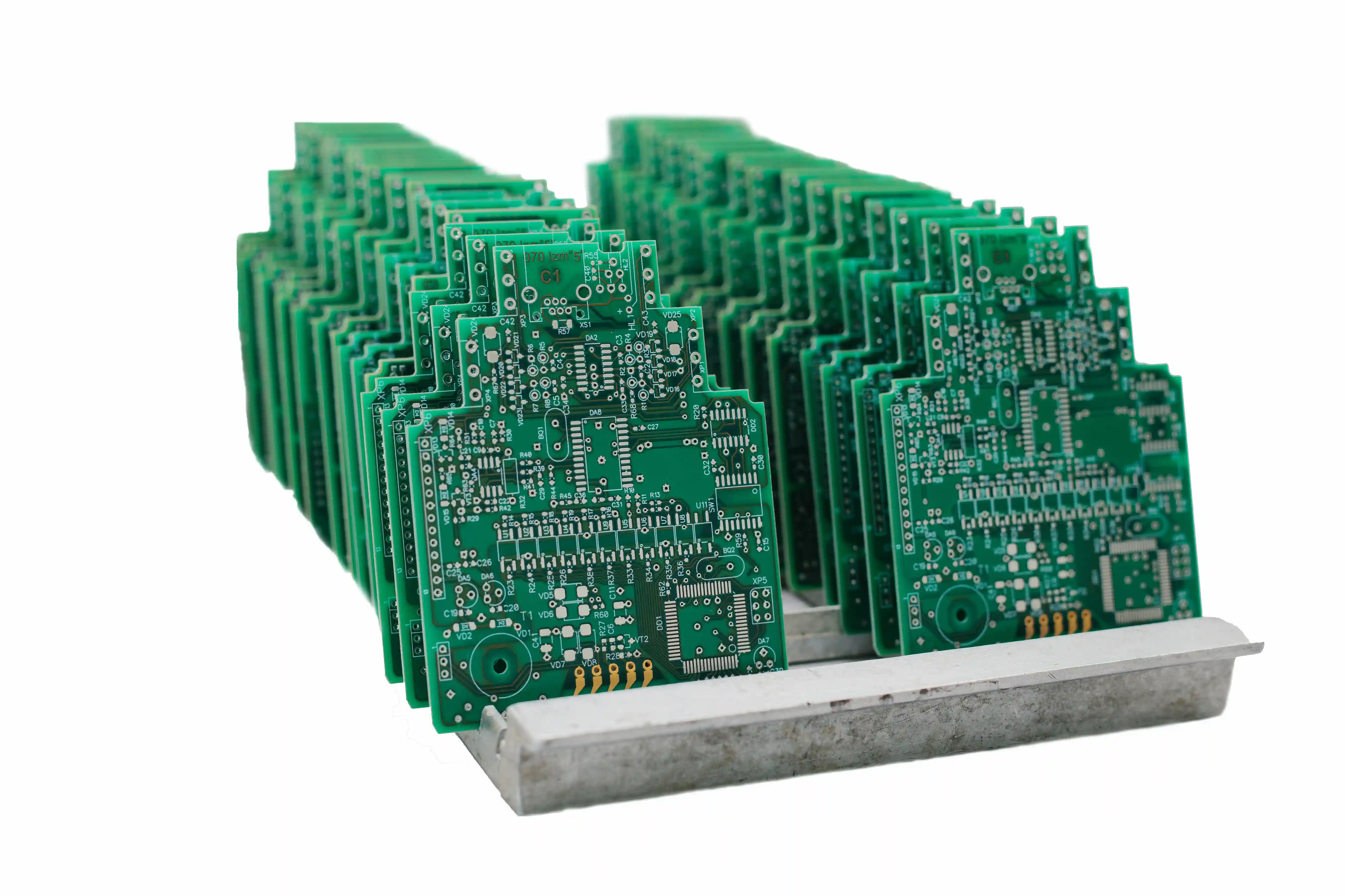
Multilayer PCB Fabrication
4 Layer PCB Manufacturing for Cleaner Routing and Better Control
PCB Insider supports 4 layer PCB manufacturing for commercial prototypes, NPI programs, and repeat production builds where routing density, plane structure, and downstream assembly readiness matter more than chasing the absolute lowest bare-board cost.
For many hardware teams, a 4-layer board is the point where the design becomes easier to route, easier to test, and easier to scale. This service is built around that specific buying intent.
Dedicated Plane StructureDFM Before ReleaseTypical 3-7 Day Lead Time
4-Layer
Signal, Ground, Power, Signal
4 Layers
Signal + Plane Architecture
3-7 Days
Typical Lead Time
100%
Electrical Test Coverage
DFM First
Release Discipline
Why Buyers Specify 4-Layer Boards
The decision is usually not about adding layers for the sake of it. It is about reducing routing compromise, stabilizing plane structure, and making the board easier to fabricate and assemble predictably.
Practical 4-Layer Stackups
A 4-layer board is often the first layout step that gives designers real control over signal routing and power distribution.
Impedance and Return Path Planning
When 4-layer designs carry faster interfaces, reference plane continuity matters as much as nominal impedance.
Prototype to Production Continuity
Many engineering teams choose 4-layer construction because it can support both first prototypes and repeat production without a redesign.
Assembly-Ready Fabrication
Pad finish, board flatness, panel strategy, and coupon planning are reviewed from a downstream PCBA perspective.
DFM Review Before Release
We focus the review on the failure points that matter most on multilayer work: annular ring margin, drill aspect ratio, solder mask clearance, copper.
Verification for Commercial Builds
Every completed panel goes through electrical testing and final inspection before shipment.
4-Layer PCB Capability Snapshot
These ranges reflect the envelope most buyers expect for practical 4-layer fabrication when the goal is controlled, repeatable bare boards rather than a marketing-only capability list.
| Service Focus | 4 layer PCB fabrication for prototype, NPI, and repeat production |
|---|---|
| Common Materials | FR-4, high-Tg FR-4, selected specialty laminates by review |
| Typical Board Thickness | 0.8 mm, 1.0 mm, 1.2 mm, 1.6 mm, and custom builds |
| Copper Weight | 0.5-2 oz standard, higher copper by engineering review |
| Min. Trace / Space | 4/4 mil standard; finer features subject to stackup and yield review |
| Min. Mechanical Drill | 0.20 mm standard production capability |
| Surface Finish | ENIG, lead-free HASL, HASL, OSP depending on application |
| Impedance Control | Single-ended and differential structures with stackup planning |
| Solder Mask | Green standard with additional colors available |
| Test Coverage | 100% electrical test on finished production panels |
| Typical Lead Time | 3-7 business days after DFM approval |
| Downstream Support | Prepared for SMT assembly, inspection, and system build workflows |
Common Fit for This Service
Embedded and Control Boards
Microcontroller, FPGA-adjacent, and mixed-signal control boards often move to 4 layers to keep routing sane while reserving dedicated planes.
Commercial Prototype Programs
A 4-layer board is a common choice when a project has moved beyond proof-of-concept and now needs a cleaner stackup for validation, certification work.
SMT Builds That Need Flatness and Consistency
Compared with crowded 2-layer layouts, a well-planned 4-layer design usually simplifies routing compromises and creates a more stable bare board input.
Bridge Production Before Full Scale-Up
If you need repeat 4-layer builds before a volume transfer is finalized, this service supports the documentation and process consistency needed.

Verification Still Matters on a Familiar Stackup
4-layer work is common, but that does not make it immune to shorts, opens, or stackup-related surprises. Electrical test coverage remains part of the release discipline.
4-Layer Fabrication Process
Multilayer work is not just a 2-layer job with extra copper. The stackup, lamination, and verification path need to be checked up front if the goal is predictable output for purchasing and PCBA.
1
File Intake and Stackup Review
We review Gerber or ODB++ data, drill files, fab notes, quantity, finish, thickness, and any impedance targets.
2
Multilayer DFM Signoff
Engineering checks copper balance, plane usage, annular ring, drill-to-copper clearance, solder mask registration, and fabrication tolerances.
3
Fabrication and Layer Registration
Inner layers are processed, laminated, drilled, plated, and patterned under controls appropriate for multilayer work.
4
Electrical Test and Shipping Release
Finished panels receive electrical verification and final inspection.
Standards and Material References
Buyers evaluating 4 layer PCB manufacturing usually care about stackup discipline, material selection, and industry rules for layout and workmanship. These references are useful starting points.
Multilayer PCB provides a concise overview of why layered constructions are used when routing density and performance expectations rise.
FR-4 remains the standard reference material family for most 4-layer commercial builds unless the design pushes into specialty laminate requirements.
IPC standards underpin many of the fabrication, design, and workmanship expectations buyers use when qualifying PCB suppliers.
Need 4-Layer Boards Ready for Assembly?
Send Gerber or ODB++ data, required thickness, finish, quantity, and any impedance targets. We can review whether your 4-layer stackup supports the electrical goal and the downstream assembly plan before the job is released.
Frequently Asked Questions
The common buying questions around 4-layer stackups, quoting, and production fit.
When should I choose 4 layer PCB manufacturing instead of 2 layers?
Choose 4 layers when routing density, EMI control, power integrity, or controlled return paths start to matter more than minimizing bare-board cost. Many designs move to 4 layers once a 2-layer layout becomes too congested or when the board needs cleaner signal behavior for commercial release.
What is the most common 4-layer PCB stackup?
A common structure is signal, ground plane, power plane, signal. The exact dielectric thickness and copper weights depend on impedance targets, board thickness, current demand, and assembly constraints. We review those details before production rather than assuming one stackup fits every design.
Can you support controlled impedance on 4-layer boards?
Yes. Controlled impedance is a common requirement on 4-layer boards for interfaces that need more predictable transmission behavior. Provide your target impedance, layer intent, finished thickness, and any material preference so the stackup can be reviewed during DFM.
Is 4 layer PCB manufacturing suitable for prototypes as well as production?
Yes. A 4-layer board is often a strong choice when you want prototype hardware that can scale into pilot or production builds without re-architecting the stackup. That continuity reduces redesign risk later in the sourcing cycle.
What files do you need to quote a 4-layer PCB order?
At minimum we need Gerber or ODB++ files, NC drill data, board thickness, copper weight, surface finish, quantity, and delivery requirement. If the board uses impedance control, include target values and any preferred stackup information.
Related Resources
Continue from fabrication planning into costing, file review, assembly, or broader service selection.
PCB Manufacturing
Broader fabrication capability beyond a single stackup target.
ExploreFR-4 PCB Manufacturing
Material-controlled standard and high-Tg rigid PCB fabrication.
ExploreLow Volume PCB Manufacturing
Short-run production for NPI, pilots, and repeat small batches.
ExplorePCB Assembly
SMT, through-hole, and mixed-technology support after fabrication.
ExploreImpedance Calculator
Check routing assumptions before releasing the board stackup.
ExploreGerber Viewer
Review manufacturing data before sending the RFQ package.
ExploreIPC-2221 Overview
Context for design rules and board-level layout decisions.
Explore