Plated Through Hole vs. Via
Plated through hole vs. via: Understand the differences between PTH and vias in PCB design. Learn when to use each type for your circuit board projects.
Here’s a detailed plated-through hole vs. via comparison.
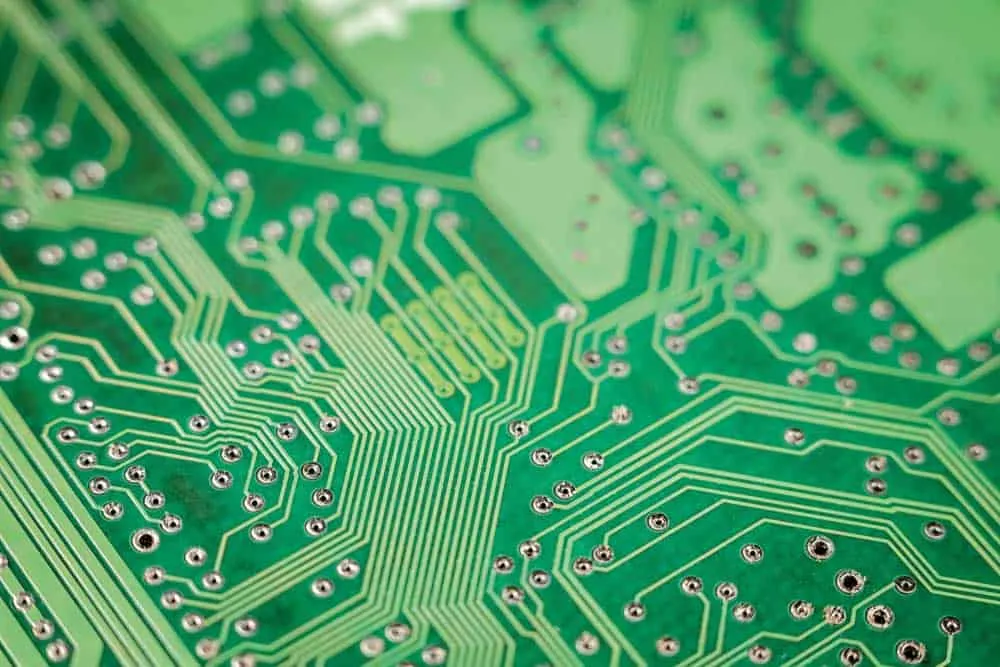
Most novice electronics engineers might look at PCBs and assume all the holes are vias or plated through holes.
Although both are holes, the terms don’t refer to the same thing.
So read this article to find out more!
What Is a Via?
A via is a hole drilled between two or more PCB conductive layers to create an electrical connection.
These connections allow trace routing between these layers for conducting electrical signals.
So vias are not necessary when dealing with a single-layer board.
But they are critical parts of multi-layered boards to enable the interconnection between copper layers.
Also, vias help increase trace density because the wiring can pass above and below other copper traces.
So while the conductive layer forms horizontal connections, vias form vertical links.
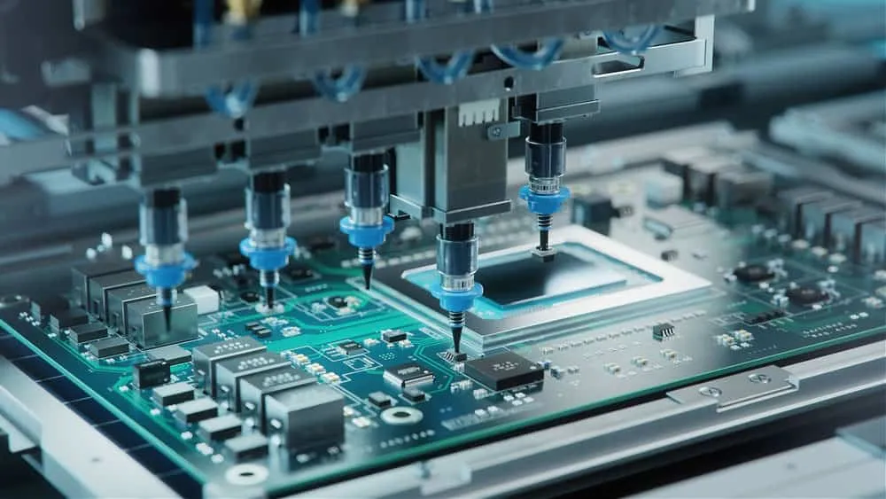
How To Create Vias
Vias begin as copper pads placed on each board layer during fabrication. After that, a hole gets drilled through the copper pad.
Then a chemical gets poured on the next layer to dissolve the epoxy.
The dissolved epoxy uncovers the hidden copper pads in the adjacent layer for drilling.
You repeat these steps until you get to the required via connectivity in the internal layers.
But after drilling, the hole walls are non-conductive. So they have to undergo electroplating to give the barrels electrical conductivity properties.
Alternatively, you can insert copper cylinders into the holes to connect the exposed copper layers.
Via Components
Although vias come in different types, they all have these three components.
Pad
A pad or annular ring is the circular copper area that links the upper and lower ends of the barrel.
Anti-pad
An anti-pad is a hole separating the barrel from the layers it should not connect to.
Barrel
Barrels are conductive tubes lined on the drilled hole created by inserting copper cylinders or electroplating.
So barrels form connections between layers.
And engineers usually use the aspect ratio (ratio of the hole diameter to length) to determine the barrel strength.
Types of Vias
The types of vias vary depending on factors like size, hole diameters, and pad shape. They include:
Through-Hole Vias
As the name suggests, these vias connect the outermost layers because they extend from top to bottom.
Also known as plated-through vias, these holes create an electrical connection between all the PCB layers.
They are the easiest and cheapest to make but can take up a lot of space.
Buried Vias
A buried via connects two or more internal metal layers without reaching the external layers.
So making them involves drilling and electroplating them in the inner layers, then covering them.
The concept enables dense copper trace routing because you can even have two or more buried vias above the other.
But this stacking creates another via type that we’ll look at below.
However, you cannot drill holes directly on the board when creating a buried via to connect three or more interior layers.
Blind Vias
Blind vias connect the upper or lower PCB layer to at least one inner layer. So the hole is blind because it doesn’t get to see the other end.
You can use mechanical or laser drilling to create these vias, then electroplate the walls to form the barrel.
Stacked Vias
Stacked vias can be blind or buried via holes layered above each other.
You can also think of them as vias connecting two adjacent layers placed above each other to form a continuous hole.
Although easier to design than staggered vias, stacked vias are costlier to fabricate because they require more precision.
Staggered Vias
Unlike stacked vias, the staggered types do not overlap.
They connect adjacent layers in a staggered manner, meaning they don’t create a continuous hole. But they connect the layers electrically.
Although more complex to design, staggered vias are cheaper to build, resulting in a less costly fabrication process.
Skip Vias
A skip via is a hole that goes through several PCB layers without electrically connecting to some layers.
The via holes can be blind, buried, or overlapping (stacked).
Compared to blind vias, skip vias can connect the outer and inner layers without linking the ones in between.
The holes can also be core vias if they link several internal layers, but not successively.
Microvias
Micro means small. So microvias are tiny vias with a drill diameter of 150 micrometers (0.15mm) or less.
But in the revised 2013 IPC standards, microvias have an aspect ratio of 1:1 or less.
And they have a depth not exceeding 250 micrometers (0.25mm).
Some people exceed the IPC 1:1 aspect ratio, but such holes can have reliability issues.
Regardless, this tiny hole size takes up less space on the board, leaving more area for trace routing.
And in addition to enabling the fabrication of dense, complex boards, microvias reduce parasitic capacitance.
So they are ideal for high-speed, high-frequency circuits.
On top of that, they allow engineers and designers to make the component layout with tinier BGA pitches.
It is vital to note you can only use laser drills to bore microvias.
This method is costlier and more complex than the mechanical drilling process. But it is safer because it reduces manufacturing defects.
Also, laser drills generate little to no residue.
Via-in-Pad
On high-density boards, it is acceptable to position vias under SMD pads.
This design enables component soldering on the surface layer.
So instead of having a hole on a microvia, blind via or through-hole via, a surface-mount pad sits above this hole.
Therefore, you can mount a BGA or SMT component directly on the via hole.
Via-in-pads eliminate the need for conventional routing of a signal trace from the component’s pad to the via.
The reduced wiring creates a miniaturized PCB form factor because it cuts the area required for routing copper traces.
Functions of Vias
Vias can serve either of the following functions.
Power Routing
Power routing requires large vias, such as the through-hole type.
So most boards have through-hole vias for power and ground-net routing to supply power to the inner layers.
But you can also use blind vias for this task.
Signal Routing
Most boards use vias holes for signal routing. Buried and blind vias are ideal for dense boards, while microvias are the best for extremely-dense PCBs.
Thermal Regulation
Some PCB components generate heat, which can damage other PCB parts if there’s no control.
Vias can help dissipate heat from these components via the inner plane layers.
Through-hole vias are the best for this task, but you can also use blind vias.
Escape Routing
Escape/fanout routing is a routing technique that directs every signal from a package to another PCB element.
For instance, you can route a package’s I/O pads to lines that can escape to the area around the die.
You can route signals from this area to the immediate surroundings outside the die.
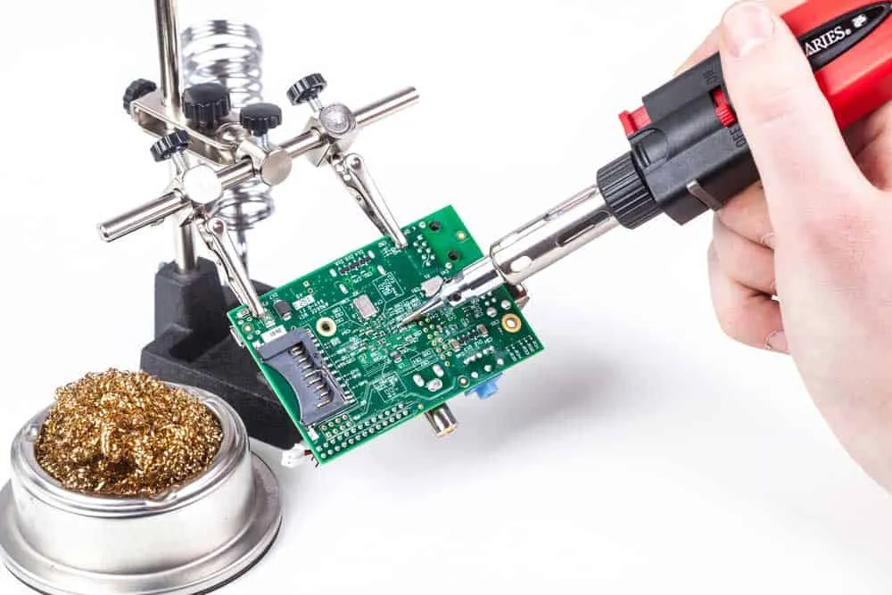
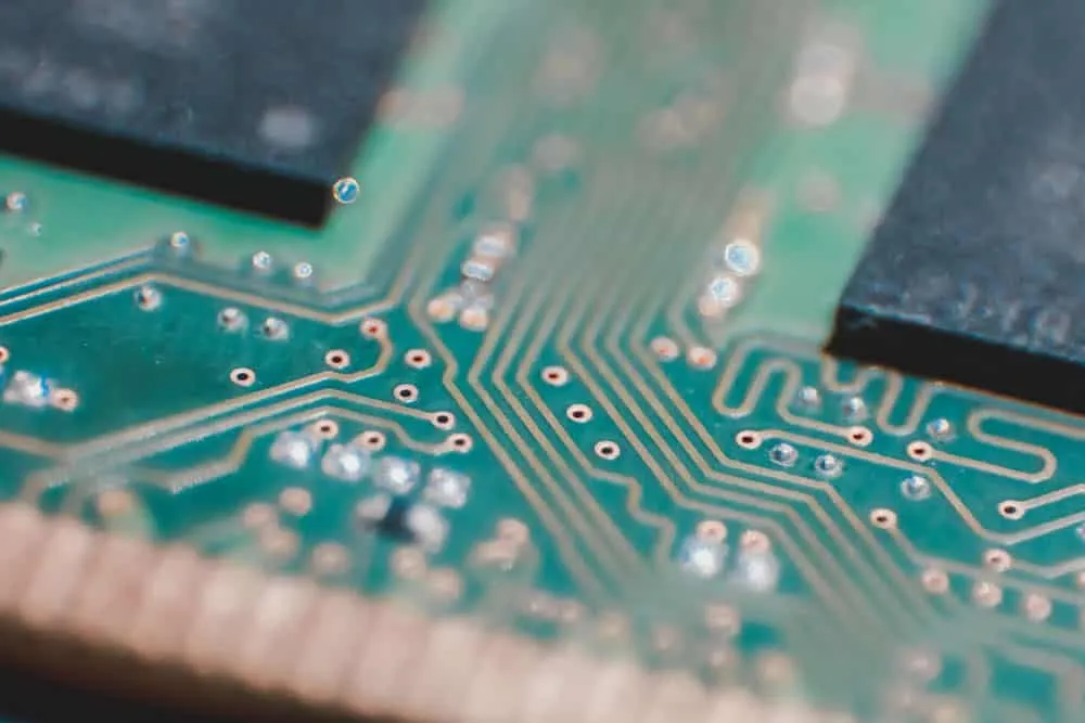
What Is a Plated Through Hole?
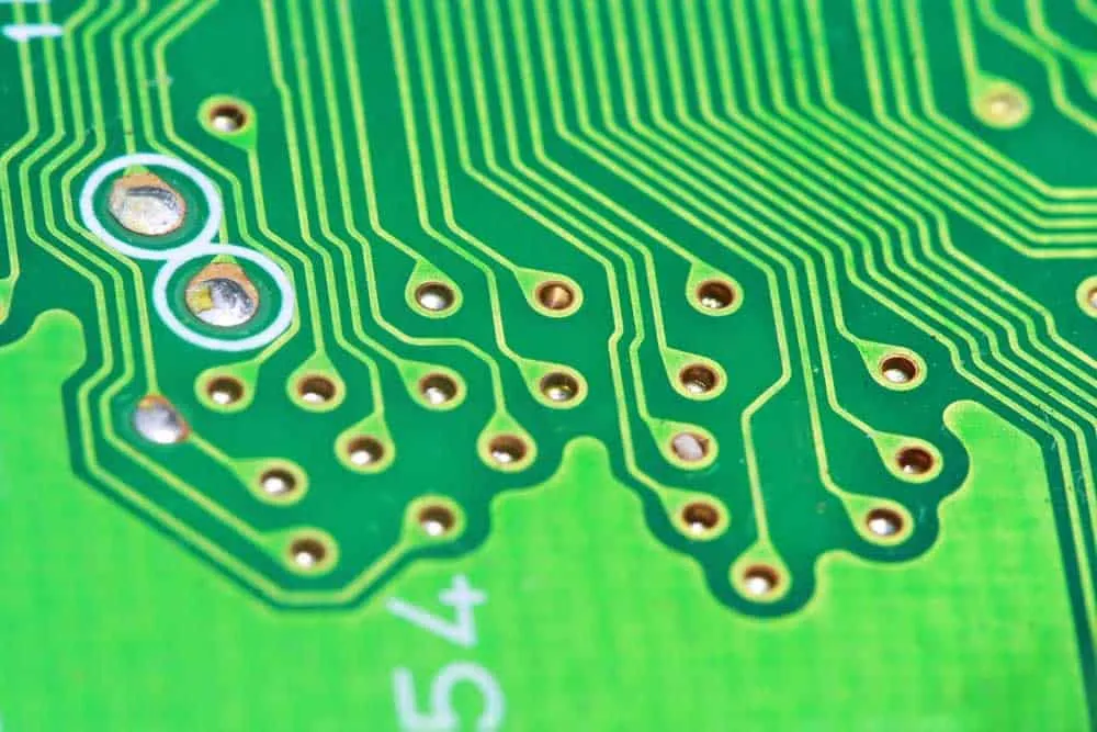
A plated through hole is a large hole drilled through a circuit board for mechanical and electrical connections.
But remember, vias only allow signal and power transmission between layers.
On the other hand, plated through holes allow signal and power connectivity, plus mechanical connections.
Also, they have a longer diameter and allow thru-hole component leads inside for soldering.
These include DIP integrated circuits, capacitors, resistors, diodes, etc.
Another critical function for plated-through holes is the castellated hole.

When you cut this board along the edge, the holes emerge as multiple plated semi-circles.
You can use these metalized edges to solder the boards in a stack. So the holes can act as connectors or fasteners.
Wrap Up
As you can see, plated through holes and vias are different structures in a PCB. The former can provide mechanical and electrical connections, while the latter only allows electrical connectivity.
And it is vital to know the differences to use the appropriate structure for its correct function.
Comment below if you found the article insightful or want to share your sentiments. We’ll be in touch for further discussion. Explore our PCB manufacturing services for multilayer boards with various via types.
Related Articles
Continue exploring similar topics

Tinning Flux vs Regular Flux
Today, we provide insights into the tinning flux vs. regular flux debate. We aim to educate you on their benefits to any typical soldering process.
SMD vs. SMT vs. THT: PCB Comparison
This article is a comparison of SMD vs. SMT. vs. THT. If you have researched the PCB assembly processes, you must have encountered acronyms like SMD, SMT, and THT.
Allegro vs. Altium: PCB Software Guide
Allegro vs. Altium: Compare features, pros, cons, and pricing of these leading PCB design tools. Find out which software best fits your design needs.
Ready to bring your PCB design to life?
Get an instant quote for your custom PCB fabrication and assembly needs.
Get Instant Quote