Conductive vs. Non-Conductive Via Fill PCB
Conductive vs. non-conductive via fill: Compare materials, costs, and applications. Learn which via fill type suits your PCB design requirements.
We’ll compare the conductive vs. non-conductive via fill PCB below.
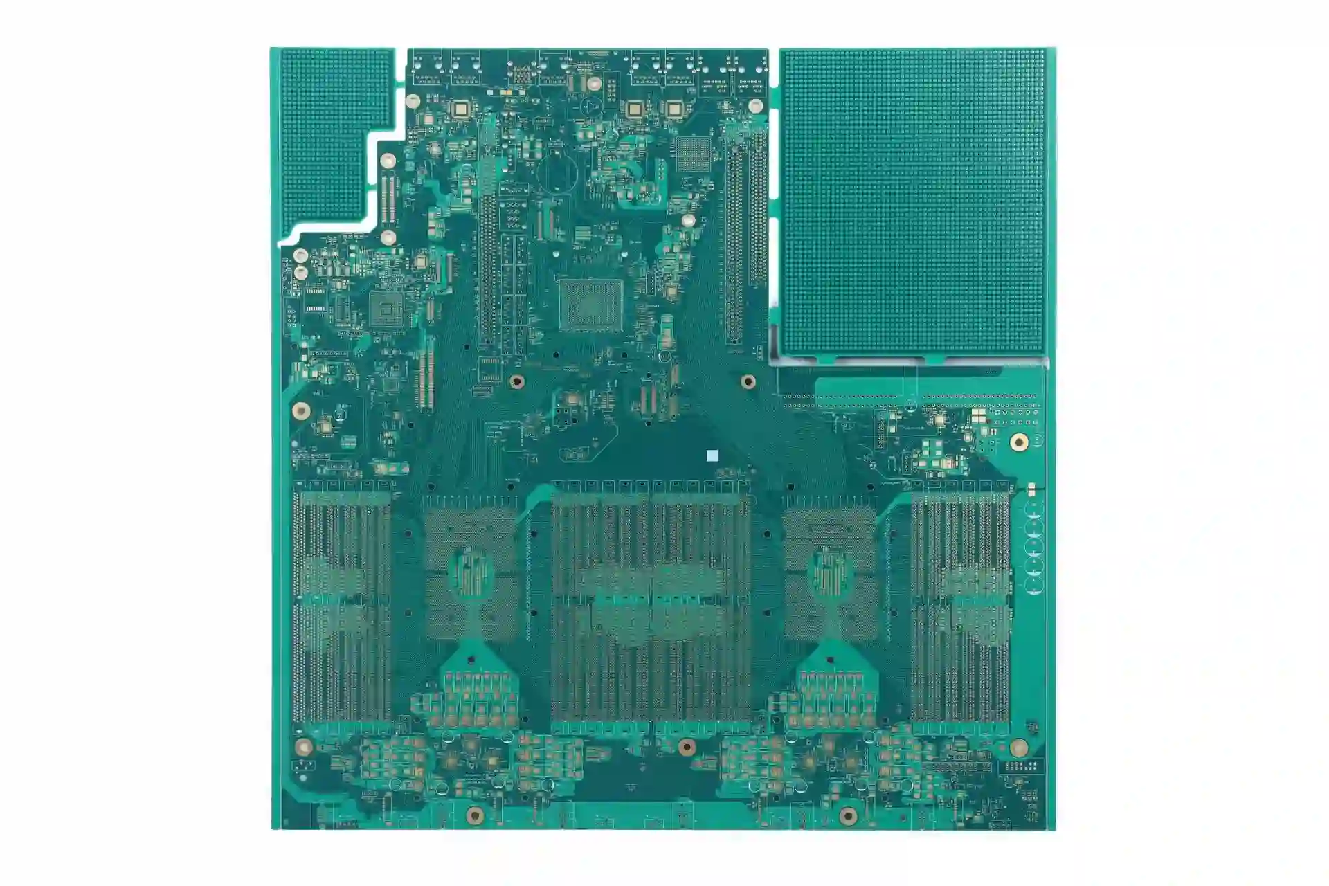
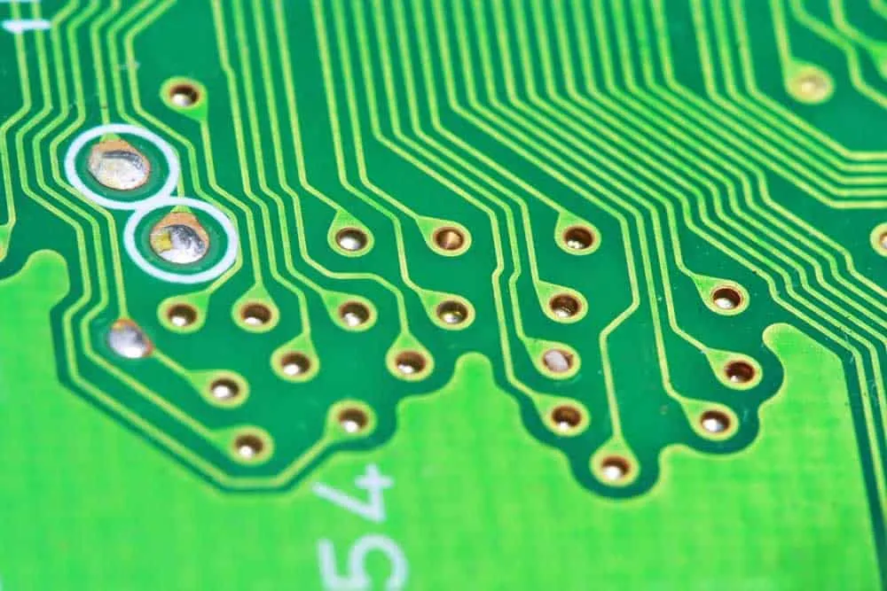
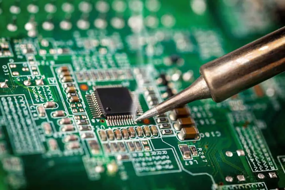
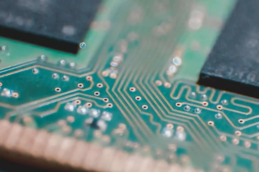
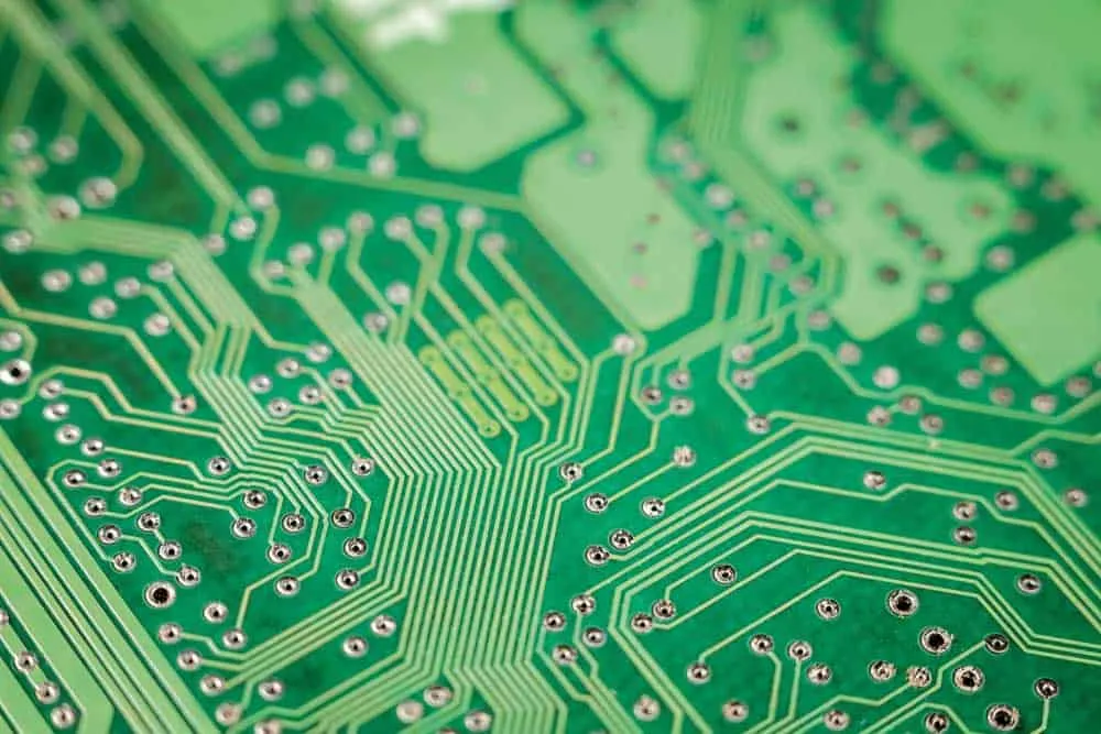
Vias are critical structures in circuit boards because they connect internal layers and enhance heat dissipation.
But they can either be empty or filled. And when filled, they can have a conductive or non-conductive material in the cavity. Take a look!
What Is a Conductive Via Fill?
Conductive via fills are PCB via holes filled with silver or copper epoxies. The primary products used for this filling are DuPont CB100 or Tatsuto AE3030 epoxy. These two materials have superb thermal and electrical properties.
So conductive via filling enables electrical signal transfer to different circuit board sections and layers. And it encompasses heat transfer for cooling purposes. For instance, integrated circuits and microprocessors can use filled vias to transfer heat to the other side.
What Is a Non-Conductive Via Fill?
Non-conductive via fills are similar to the conductive type when considering the fabrication process. But the material used is different. It is non-conductive.
So the work of this filled via is to prevent via hole contamination, especially by solder. Additionally, the filler material provides structural support to the copper pad that seals the hole.

Benefits of Via Filling
The combined benefits of conductive and non-conductive via filling include the following.
- - Reliable surface mounts (strengthens pad attachments)
- Reduced electromagnetic interference
- Short high-frequency design routes for bypassing capacitors
- Better electrical and thermal conductivity
- Increased assembly yields
- Eliminates high-speed design constraints, such as low inductance
- Reduces the chances of trapping air or liquids in the board, increasing reliability
- Cuts the PCB size and number of layers
Via Tenting vs. Via Plugging vs. Active Pads
When fabricating vias in circuit boards, there are three ways to handle them.
Conductive vs. Non-Conductive Via Fill PCB: Via Tenting
A tent is a cover that shields against exterior elements. So via-hole tenting involves using a solder mask layer to cover the cavity and its annular ring.
This masking is affordable because it does not increase costs in the board’s production process.
However, there is no guarantee the hole will remain covered; the solder mask can peel off. So while the primary aim of via tenting is to prevent exposure to the elements and accidental shorting, it is not as effective.
But tiny vias with diameters lower than 12 mils have higher chances of remaining tented. For larger ones, it is better to fill and seal them.
Conductive vs. Non-Conductive Via Fill PCB: Via Plugging
Also known as mask-plugged vias, via plugging is the same as non-conductive via filling. It involves plugging the hole, securing the annular ring, and sealing the top part using a solder mask layer.
Conductive vs. Non-Conductive Via Fill PCB: Active Pads
Active pads or via-in-pads are more typical in modern BGA packages because they make them compact.
PCB fabricators mostly use dog bone land patterns to drill the vias directly in the BGA pads. This pattern ensures the vias receive electrical signals from the BGA, sending them to different board layers.
Active pads usually have vias filled with conductive materials underneath. These copper or silver fillings enhance the hole’s electrical performance for reliable signal transmission to the internal layers.
How To Fabricate Filled Vias

The manufacturing process for both filled vias is the same and includes the following steps.
Via Drilling
You can drill the hole using either mechanical or laser drilling methods. The selected process should be the most suitable for your production volume, hole depth, and operation costs.
Via Cleaning
After drilling, clean the holes to eliminate all the debris. You can use mechanical (abrasive) and chemical methods for this step. The alternative is to use a brush and solvent. Afterward, inspect the board to ensure the vias have an even copper plating.
Via Filling
You can fill the vias using conductive or non-conductive materials (depending on your requirements). This filling process requires pressure and vacuum to eliminate excessive resin and gap formation.
Filled Via Planarization
Planarization is a mechanical process involving brushing the filled vias to eliminate the excess resin. And it smoothens the copper surface, as well. The result is a uniform surface, which paves the way for over-plating.
Over-Plating
Over-plating involves covering the filled via with copper to seal the materials inside. So it creates a flat surface or pad for soldering electronic components.
Conductive vs. Non-Conductive Via Fill: Electrical Conductivity
The primary difference between these two via-filling methods is electrical conductivity. The silver and copper epoxies used for conductive filling provide good electrical performance through the hole.
So you can use the filled via to transfer electrical signals from one layer to the other.
On the other hand, non-conductive via fills don’t have conductive epoxy inside. But it doesn’t mean they are not conducive. The barrels still have a thin copper plating to connect the layers.
So you can use this via hole if you don’t need to transmit high electrical current levels. Conductive elements in vias only increase the flow of electrons.
Conductive vs. Non-Conductive Via Fill: Thermal Conductivity
Non-conductive vias are not the best for thermal vias because the materials used are bad conductors.
Conductive vs. Non-Conductive Via Fill: Solder Bridging
A solder bridge defines a situation where two points on a PCB inadvertently connect electrically. This connection can create electric shocks that can burn components. So to prevent such occurrences, consider using non-conductive via fills.
Conductive vs. Non-Conductive Via Fill: CTE Value Matching
CTE (Coefficient of Thermal Expansion) refers to the fractional length increase as temperatures rise.
With vias, you must match the CTE of the filling material and the surrounding laminate to avoid stress fracturing.
These fractures usually occur if the board undergoes repeated heating and cooling cycles.
Generally, non-conductive epoxy is a safer bet when considering CTE values matching. It creates a more reliable structure that matches the laminate’s CTE.
How To Pick Between Conductive and Non-Conductive Filled Vias
Consider these factors when selecting between conductive and non-conductive filled vias.
- - Think of the price: Each conductive and non-conductive epoxy filling has a different cost. So pick the most affordable material that is ideal and optimal for the application area.
- Consider the application: The application requirements are the most critical when selecting the via fill. So always pick the best material for electrical performance, cooling, insulating, or eliminating hole contamination.
- Simplify the board design: Ultimately, simplicity leads to reliability. So avoid complicated PCB designs when laying out these vias.
Wrap Up
In conclusion, the conductivity or non-conductivity of the material in the hole determines the properties of the via.
And as you can see, these properties make the vias suitable for different application areas.
That marks the end of this article. Comment your sentiments below to let us know your thoughts or if we left something out. Need via filling for your boards? Check out our PCB manufacturing services and assembly capabilities.
Related Articles
Continue exploring similar topics

Tinning Flux vs Regular Flux
Today, we provide insights into the tinning flux vs. regular flux debate. We aim to educate you on their benefits to any typical soldering process.
SMD vs. SMT vs. THT: PCB Comparison
This article is a comparison of SMD vs. SMT. vs. THT. If you have researched the PCB assembly processes, you must have encountered acronyms like SMD, SMT, and THT.
Allegro vs. Altium: PCB Software Guide
Allegro vs. Altium: Compare features, pros, cons, and pricing of these leading PCB design tools. Find out which software best fits your design needs.
Ready to bring your PCB design to life?
Get an instant quote for your custom PCB fabrication and assembly needs.
Get Instant Quote