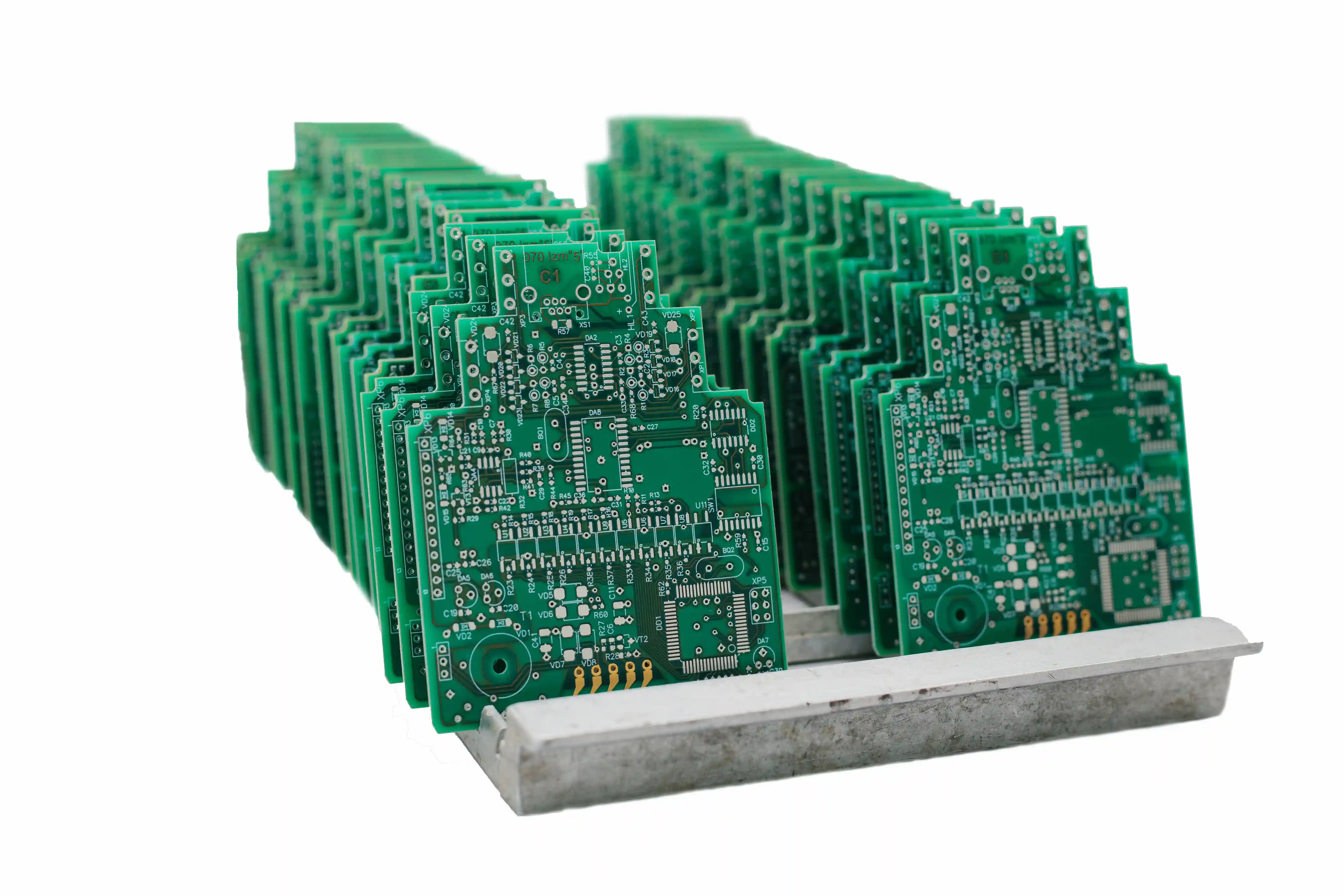
1 Layer PCB Fabrication
Single Sided PCB Manufacturing for Simple, Cost-Driven Electronics
PCB Insider supports single sided PCB manufacturing for buyers who need practical one-layer fabrication for LED boards, appliance controls, power interfaces, and legacy electronics where simple routing and cost discipline matter most.
A 1 layer board is not automatically the best choice just because it is cheaper to build. This service is designed to help teams keep the product simple without introducing routing compromises, assembly headaches, or supply instability later.
Cost-Focused ConstructionDFM Before ReleaseTypical 3-5 Day Lead Time
1 Layer
Practical, Low-Complexity PCB Build
1 Layer
Cost-Focused Construction
3-5 Days
Typical Lead Time
DFM First
Release Discipline
Assembly Ready
Downstream Support
Why Buyers Still Choose Single Sided Boards
One-layer construction is still commercially relevant because it can remove unnecessary process cost from the product. The real decision is whether the design stays practical after simplifying the board architecture.
Built for Cost-Sensitive Electronics
Single sided boards remain a practical choice when the circuit is simple, component density is manageable, and the program needs the lowest sensible.
Ideal for Straightforward Routing
One-layer construction works well for LED lighting, power distribution, adapter boards, appliance controls, and simple industrial interfaces where routing.
DFM Review Before Release
We review copper spacing, annular ring where drilled holes are used, pad sizes, board outline, surface finish, and panel strategy before production so.
Practical Material and Finish Selection
The right specification depends on actual use. We help align FR-4 thickness, copper weight, solder mask, and finish with current demand, assembly method.
Prototype Through Repeat Builds
Single sided PCB manufacturing is often used for ongoing commercial products, not only prototypes.
Assembly-Aware Fabrication
Even a basic board benefits from fabrication choices that support later soldering, depanelization, labeling, and incoming inspection.
Commercial Fit and Capability Snapshot
Single sided PCB manufacturing is usually purchased for straightforward circuits, but it still needs disciplined specifications. Industry baseline practices such as IPC workmanship guidance and layout intent shaped by printed circuit board construction fundamentals still matter when the goal is reliable supply, not just a low unit price.
| Service focus | Single sided PCB fabrication for simple and cost-driven electronics |
|---|---|
| Construction | 1 copper layer on rigid laminate; no plated interconnect required |
| Typical materials | FR-4, high-Tg FR-4, aluminum for selected applications by review |
| Typical thickness | 0.8 mm, 1.0 mm, 1.2 mm, 1.6 mm, and custom builds |
| Copper weight | 0.5-2 oz standard, heavier copper subject to review |
| Common finishes | HASL, lead-free HASL, OSP, ENIG based on assembly needs |
| Typical applications | LED modules, power boards, chargers, appliances, simple controls |
| Lead time | Typically 3-5 business days after DFM approval |
| Volume profile | Prototype, NPI, service spares, and repeat production runs |
| Downstream fit | Prepared for manual, wave, or selective solder assembly workflows |
Buyer Questions This Service Solves
When single sided is the right commercial choice
Buyers usually choose 1 layer boards to reduce cost, simplify supply, and keep products manufacturable at scale.
What can quietly drive hidden cost back in
A board that is too aggressively simplified can become harder to route, larger than necessary, or more labor-intensive to assemble.
How to avoid false economy in specifications
The lowest-cost finish or thinnest copper is not always the best choice.
What procurement teams compare
Commercial buyers typically compare price stability, file review quality, practical lead times, and whether the supplier can support fabrication.
Typical Use Cases
LED and Lighting Circuits
Many LED driver auxiliaries, indicator boards, and basic lighting modules fit single sided construction when thermal, current, and routing needs remain modest.
Appliance and Consumer Control Boards
Simple timer boards, button interfaces, charger auxiliaries, and low-complexity household electronics often use one-layer boards to keep BOM.
Power and Interface Subboards
Adapter boards, relay boards, terminal interfaces, and power distribution subassemblies can remain highly manufacturable with a single copper layer.
Service Spares and Legacy Products
Older products frequently rely on simple board architectures that still need dependable repeat supply.
Where 1 Layer Often Wins
If the circuit can stay on one copper layer with sensible spacing, accessible solder joints, and a reasonable outline, the program often benefits from lower fabrication cost and simpler purchasing. If it cannot, the right decision is usually to move to a 2-layer or 4-layer service early rather than force the product into a weaker layout.
Process Flow for Single Sided PCB Manufacturing
The manufacturing route is simpler than multilayer PCB work, but the release still benefits from good file control, panel planning, and inspection discipline.
1
Review files and commercial targets
We review Gerber or ODB++ data, quantity, target lead time, thickness, copper weight, finish, and any assembly notes so the quotation reflects the real.
2
Perform single-layer DFM checks
Engineering checks trace and clearance, pad geometry, drill usage, copper-to-edge spacing, solder mask openings, and panel handling details that affect.
3
Fabricate and finish the boards
Panels move through imaging, etching, drilling where required, solder mask, legend, surface finish, profiling, and lot control under the selected process.
4
Inspect, pack, and release for assembly
Finished boards are inspected and packed to support incoming verification and downstream soldering.
Quote-Ready Support
Release Simple Boards Without Treating Them Casually
The board may be simple, but the buying decision still affects cost, lead time, yield, and downstream assembly performance. Send over your fabrication package and target volume, and we can review whether single sided PCB manufacturing is truly the right fit or whether a small move in board architecture would create a better commercial result.
RFQ Checklist
- Gerber or ODB++ files plus drill data
- Board thickness, copper weight, and finish requirement
- Quantity, forecast, and target delivery window
- Assembly notes if the product will be soldered after fabrication
Frequently Asked Questions
Common questions from buyers comparing one-layer PCB options with broader fabrication or assembly services.
When should I choose single sided PCB manufacturing instead of a 2-layer board?
Choose single sided construction when the circuit is simple enough to route on one copper layer without awkward compromises, the board size remains practical, and the commercial goal is cost control. If jumpers, oversized outlines, or heavy assembly workarounds start appearing, a 2-layer board may be the better value.
What products commonly use single sided PCBs?
Common examples include LED modules, charger auxiliaries, simple power boards, relay interfaces, appliance controls, and legacy industrial electronics. The best fit is usually a straightforward circuit with manageable component density and limited routing crossover needs.
Can single sided PCB manufacturing still support production volumes?
Yes. Single sided boards are often used in repeat production because the construction is simple and cost-effective. What matters is stable documentation, realistic specifications, and a supplier that can keep yield and lead time consistent across repeat orders.
Which surface finish is best for a single sided PCB?
That depends on the assembly process, shelf-life needs, and pad geometry. HASL and lead-free HASL are common value-focused choices, while OSP or ENIG may make sense when flatness, storage, or downstream process requirements justify them.
What files do you need to quote a single sided PCB order?
At minimum we need Gerber or ODB++ data, drill files if applicable, board thickness, copper weight, surface finish, quantity, and delivery target. Assembly drawings or notes are also useful when the board will move into soldering after fabrication.
Can you support assembly after single sided PCB fabrication?
Yes. If the product also needs SMT, through-hole, selective solder, or box build integration, we can align the fabrication release with the downstream manufacturing plan so the board is specified for the actual assembly process.
Related Services and Tools
Use these links to compare adjacent manufacturing options or prepare a cleaner RFQ package.
PCB Manufacturing
Broader fabrication support across multilayer, HDI, flex, and specialty boards.
ExplorePCB Prototype
Quick-turn prototype options when schedule matters as much as board simplicity.
ExplorePCB Assembly
Add SMT, through-hole, coating, and test support after fabrication.
ExplorePCB Cost Estimator
Benchmark how board choices can affect prototype and production cost.
ExploreGerber Viewer
Review manufacturing data before sending the RFQ package.
ExploreIPC-2221 Overview
Reference common PCB design rules that influence manufacturability.
Explore